

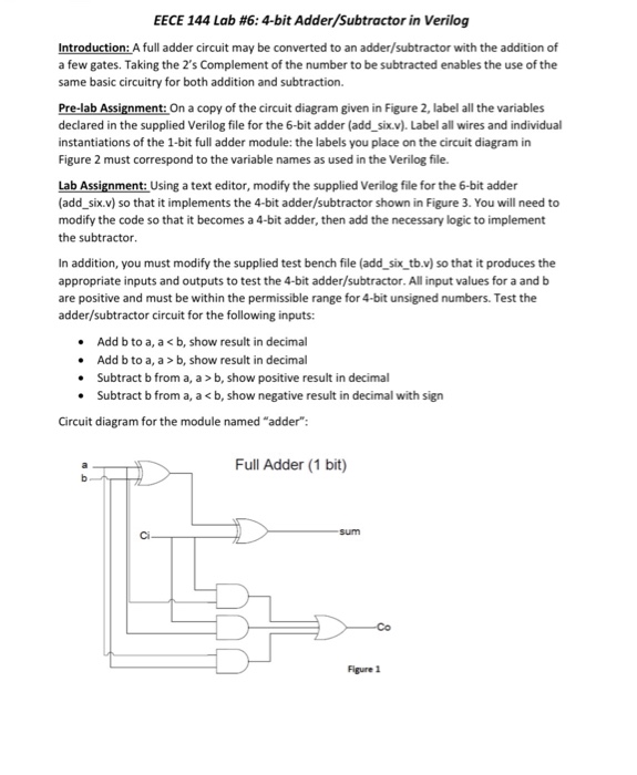
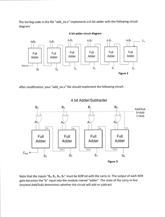
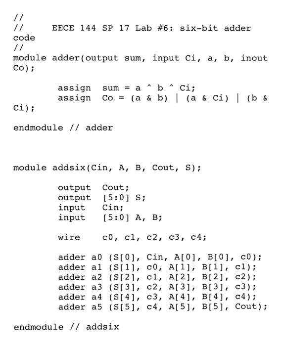
EECE 144 Lab #6: 4-bit Adder/Subtractor in Verilog Introduction: A full adder circuit may be converted...
Fantastic news! We've Found the answer you've been seeking!
Question:

Transcribed Image Text:
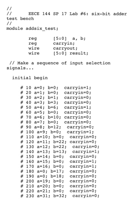
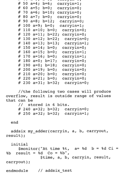
EECE 144 Lab #6: 4-bit Adder/Subtractor in Verilog Introduction: A full adder circuit may be converted to an adder/subtractor with the addition of a few gates. Taking the 2's Complement of the number to be subtracted enables the use of the same basic circuitry for both addition and subtraction. Pre-lab Assignment: On a copy of the circuit diagram given in Figure 2, label all the variables declared in the supplied Verilog file for the 6-bit adder (add_six.v). Label all wires and individual instantiations of the 1-bit full adder module: the labels you place on the circuit diagram in Figure 2 must correspond to the variable names as used in the Verilog file. Lab Assignment: Using a text editor, modify the supplied Verilog file for the 6-bit adder (add_six.v) so that it implements the 4-bit adder/subtractor shown in Figure 3. You will need to modify the code so that it becomes a 4-bit adder, then add the necessary logic to implement the subtractor. In addition, you must modify the supplied test bench file (add_six_tb.v) so that it produces the appropriate inputs and outputs to test the 4-bit adder/subtractor. All input values for a and b are positive and must be within the permissible range for 4-bit unsigned numbers. Test the adder/subtractor circuit for the following inputs: • Add b to a, a <b, show result in decimal • Add b to a, a > b, show result in decimal • Subtract b from a, a>b, show positive result in decimal • Subtract b from a, a <b, show negative result in decimal with sign Circuit diagram for the module named "adder": 3 Full Adder (1 bit) sum -Co Figure 1 The Verilog code in the file "add_six.v" implements a 6-bit adder with the following circuit diagram: Cout AB Cout Full Adder So B₂ A4B₁ Full Adder Full Adder S4 6 bit adder circuit diagram A₂B₁ B₂ Full Adder $₂ Full Adder A₂B₂ After modification, your "add_six.v" file should implement the following circuit: S₂ Full Adder 4 bit Adder/Subtracter B₁ Full Adder A₁B₁ Cout Full Adder S₁ $₁ Bo Full Adder Cout Figure 3 Figure 2 AB₂ So Full Adder Add/Sub 0 Add 1=Sub Note that the inputs "B, B₁, B2, B3" must be XOR'ed with the carry-in. The output of each XOR gate becomes the "b" input into the module named "adder". The state of the carry-in line (marked Add/Sub) determines whether the circuit will add or subtract. Hints: 1. You must define the wires needed to connect the outputs of the four additional XOR gates to the inputs of the Full Adders. 2. The output wire vector for "result" in the test bench program can be declared as signed or unsigned, the default is unsigned if not specified. If declared as unsigned, then a negative result will not be interpreted as a negative number (2's complement) and your displayed output will be incorrect. To declare as signed, use "wire signed" instead of "wire." Signoff #1: Demonstrate proper operation of your Verilog program to your lab instructor. Submit the following items with your lab report: • Printouts of your modified "add_six.v" and "add_six_tb.v" files. • Copy of the circuit diagram in Figure 3 with all components labeled according to your Verilog program. • Screenshot of your iVerilog simulation results. Lab report submissions: The report for this lab is due at the start of next week's lab session. Submit a hard copy of your report, one copy per group. Refer to the "Lab Guidelines/Report Format" document posted on Blackboard for more information. // // code EECE 144 SP 17 Lab #6: six-bit adder module adder(output sum, input Ci, a, b, inout Co); Ci); assign sum = a^ b^ Ci; assign Co= (a & b) | (a & Ci) | (b & endmodule // adder module addsix (Cin, A, B, Cout, S); output Cout; output input Cin; input wire [5:0] S; [5:0] A, B; c0, c1, c2, c3, c4; adder a0 (S[0], Cin, A[0], B[0], 0); adder al (S[1], c0, A[1], B[1], cl); adder a2 (S[2], cl, A[2], B[2], C2); adder a3 (S[3], c2, A[3], B[3], c3); adder a4 (S[4], c3, A[4], B[4], adder a5 (S[5], c4, A[5], B[5], endmodule // addsix 4); Cout); // EECE 144 SP 17 Lab # 6: six-bit adder test bench // module addsix_test; reg reg wire wire [5:0] a, b; carryin; carryout; [5:0] result; // Make a sequence of input selection signals... initial begin # 10 a=0; b=0; carryin=1; # 20 a=1; b=0; #30 a 2; b=1; # 40 a=3; b=3; # 50 a=4; b=6; # 60 a=5; b=0; # 70 a=6; b=10; # 80 a=7; b=0; # 90 a=8; b= 12; #100 a 9; b=0; # 110 a 10; b=0; # 120 a=11; b=22; # 130 a 12; b=22; # 140 a13; b=13; # 150 a 14; b=0; # 160 a 15; b=0; # 170 a 16; b=0; # 180 a=0; b=17; # 190 a=0; b=18; # 200 a 19; b=0; # 210 a=20; b=0; # 220 a 21; b=0; # 230 a=31; b=32; carryin=0; carryin=0; carryin=0; carryin=1; carryin=0; carryin=0; carryin=0; carryin=0; carryin=1; carryin=0; carryin=0; carryin=0; carryin=1; carryin=0; carryin=1; carryin=1; carryin=0; carryin=0; carryin=0; carryin=0; carryin=0; carryin=0; # 50 a=4; b=6; carryin=1; # 60 a=5; b=0; carryin=0; # 70 a=6; b=10; carryin=0; # 80 a=7; b=0; carryin=0; #90 a 8; b=12; carryin=0; # 100 a 9; b=0; carryin=1; # 110 a 10; b=0; carryin=0; # 120 a 11; b=22; carryin=0; # 130 a 12; b=22; carryin=0; # 140 a 13; b=13; carryin=1; #150 a 14; b=0; carryin=0; # 160 a 15; b=0; carryin=1; # 170 a 16; b=0; carryin=1; # 180 a=0; b=17; carryin=0; #190 a=0; b=18; carryin=0; #200 a 19; b=0; carryin=0; # 210 a 20; b=0; carryin=0; # 220 a 21; b=0; carryin=0; # 230 a 31; b=32; carryin=0; //the following two cases will produce overflow, result is outside range of values that can be // stored in 6 bits. #240 a=32; b=32; carryin=0; # 250 a=32; b=32; carryin=1; end addsix my_adder (carryin, a, b, carryout, result); initial $monitor ("At time t, a=%d b = %d Ci = Co= %b", $time, a, b, carryin, result, %b result = %d carryout); endmodule // addsix_test EECE 144 Lab #6: 4-bit Adder/Subtractor in Verilog Introduction: A full adder circuit may be converted to an adder/subtractor with the addition of a few gates. Taking the 2's Complement of the number to be subtracted enables the use of the same basic circuitry for both addition and subtraction. Pre-lab Assignment: On a copy of the circuit diagram given in Figure 2, label all the variables declared in the supplied Verilog file for the 6-bit adder (add_six.v). Label all wires and individual instantiations of the 1-bit full adder module: the labels you place on the circuit diagram in Figure 2 must correspond to the variable names as used in the Verilog file. Lab Assignment: Using a text editor, modify the supplied Verilog file for the 6-bit adder (add_six.v) so that it implements the 4-bit adder/subtractor shown in Figure 3. You will need to modify the code so that it becomes a 4-bit adder, then add the necessary logic to implement the subtractor. In addition, you must modify the supplied test bench file (add_six_tb.v) so that it produces the appropriate inputs and outputs to test the 4-bit adder/subtractor. All input values for a and b are positive and must be within the permissible range for 4-bit unsigned numbers. Test the adder/subtractor circuit for the following inputs: • Add b to a, a <b, show result in decimal • Add b to a, a > b, show result in decimal • Subtract b from a, a>b, show positive result in decimal • Subtract b from a, a <b, show negative result in decimal with sign Circuit diagram for the module named "adder": 3 Full Adder (1 bit) sum -Co Figure 1 The Verilog code in the file "add_six.v" implements a 6-bit adder with the following circuit diagram: Cout AB Cout Full Adder So B₂ A4B₁ Full Adder Full Adder S4 6 bit adder circuit diagram A₂B₁ B₂ Full Adder $₂ Full Adder A₂B₂ After modification, your "add_six.v" file should implement the following circuit: S₂ Full Adder 4 bit Adder/Subtracter B₁ Full Adder A₁B₁ Cout Full Adder S₁ $₁ Bo Full Adder Cout Figure 3 Figure 2 AB₂ So Full Adder Add/Sub 0 Add 1=Sub Note that the inputs "B, B₁, B2, B3" must be XOR'ed with the carry-in. The output of each XOR gate becomes the "b" input into the module named "adder". The state of the carry-in line (marked Add/Sub) determines whether the circuit will add or subtract. Hints: 1. You must define the wires needed to connect the outputs of the four additional XOR gates to the inputs of the Full Adders. 2. The output wire vector for "result" in the test bench program can be declared as signed or unsigned, the default is unsigned if not specified. If declared as unsigned, then a negative result will not be interpreted as a negative number (2's complement) and your displayed output will be incorrect. To declare as signed, use "wire signed" instead of "wire." Signoff #1: Demonstrate proper operation of your Verilog program to your lab instructor. Submit the following items with your lab report: • Printouts of your modified "add_six.v" and "add_six_tb.v" files. • Copy of the circuit diagram in Figure 3 with all components labeled according to your Verilog program. • Screenshot of your iVerilog simulation results. Lab report submissions: The report for this lab is due at the start of next week's lab session. Submit a hard copy of your report, one copy per group. Refer to the "Lab Guidelines/Report Format" document posted on Blackboard for more information. // // code EECE 144 SP 17 Lab #6: six-bit adder module adder(output sum, input Ci, a, b, inout Co); Ci); assign sum = a^ b^ Ci; assign Co= (a & b) | (a & Ci) | (b & endmodule // adder module addsix (Cin, A, B, Cout, S); output Cout; output input Cin; input wire [5:0] S; [5:0] A, B; c0, c1, c2, c3, c4; adder a0 (S[0], Cin, A[0], B[0], 0); adder al (S[1], c0, A[1], B[1], cl); adder a2 (S[2], cl, A[2], B[2], C2); adder a3 (S[3], c2, A[3], B[3], c3); adder a4 (S[4], c3, A[4], B[4], adder a5 (S[5], c4, A[5], B[5], endmodule // addsix 4); Cout); // EECE 144 SP 17 Lab # 6: six-bit adder test bench // module addsix_test; reg reg wire wire [5:0] a, b; carryin; carryout; [5:0] result; // Make a sequence of input selection signals... initial begin # 10 a=0; b=0; carryin=1; # 20 a=1; b=0; #30 a 2; b=1; # 40 a=3; b=3; # 50 a=4; b=6; # 60 a=5; b=0; # 70 a=6; b=10; # 80 a=7; b=0; # 90 a=8; b= 12; #100 a 9; b=0; # 110 a 10; b=0; # 120 a=11; b=22; # 130 a 12; b=22; # 140 a13; b=13; # 150 a 14; b=0; # 160 a 15; b=0; # 170 a 16; b=0; # 180 a=0; b=17; # 190 a=0; b=18; # 200 a 19; b=0; # 210 a=20; b=0; # 220 a 21; b=0; # 230 a=31; b=32; carryin=0; carryin=0; carryin=0; carryin=1; carryin=0; carryin=0; carryin=0; carryin=0; carryin=1; carryin=0; carryin=0; carryin=0; carryin=1; carryin=0; carryin=1; carryin=1; carryin=0; carryin=0; carryin=0; carryin=0; carryin=0; carryin=0; # 50 a=4; b=6; carryin=1; # 60 a=5; b=0; carryin=0; # 70 a=6; b=10; carryin=0; # 80 a=7; b=0; carryin=0; #90 a 8; b=12; carryin=0; # 100 a 9; b=0; carryin=1; # 110 a 10; b=0; carryin=0; # 120 a 11; b=22; carryin=0; # 130 a 12; b=22; carryin=0; # 140 a 13; b=13; carryin=1; #150 a 14; b=0; carryin=0; # 160 a 15; b=0; carryin=1; # 170 a 16; b=0; carryin=1; # 180 a=0; b=17; carryin=0; #190 a=0; b=18; carryin=0; #200 a 19; b=0; carryin=0; # 210 a 20; b=0; carryin=0; # 220 a 21; b=0; carryin=0; # 230 a 31; b=32; carryin=0; //the following two cases will produce overflow, result is outside range of values that can be // stored in 6 bits. #240 a=32; b=32; carryin=0; # 250 a=32; b=32; carryin=1; end addsix my_adder (carryin, a, b, carryout, result); initial $monitor ("At time t, a=%d b = %d Ci = Co= %b", $time, a, b, carryin, result, %b result = %d carryout); endmodule // addsix_test
Expert Answer:

Related Book For 

Digital Systems Design Using Verilog
ISBN: 978-1285051079
1st edition
Authors: Charles Roth, Lizy K. John, Byeong Kil Lee
Posted Date:
Students also viewed these electrical engineering questions
-
With the addition of five pairs of observations(18,000, 39.2), (22,400, 27.9), (24,210, 22.3), (5,400, 11.7), and (9,340, 32.5)to the data in Problem 3 in Chapter 5, the accompanying computer output...
-
Prove that everyNFA can be converted to an equivalent one that has a single accept state.
-
Solve Example 5.3 with the addition of a heat exchanger at each stage so as to maintain isothermal operation of the absorber at (a) 125F (b) 150oF What is the effect of temperature on absorption in...
-
31. Which combination of the compounds and their geometry are correct h) CIF, - V-shaped e) CIF, - Tshaped OB. a HeCl, - linoar 24. Which of the following havea bond angle smaller than tetrahodral...
-
Substantial equivalency refers to a. An auditors tendency not to believe managements assertions without sufficient corroboration. b. Providing consulting work for another firms audit client in...
-
Losses have been incurred at Millard Corporation for some time. In an effort to isolate the problem and improve the companys performance, management has requested that the monthly income statement be...
-
Apply the marketing-myopia concept to print media, magazines, and newspapers. What is the implication?
-
This case includes data from The Shaw Group, Inc. annual report for the year ended August 31, 2010. Assets acquired under capital leases, net of accumulated depreciation, were $ 1.6 million and $ 2.0...
-
a.) The following questions refer to the optical cavity in the diagram below. It is excited by a variable frequency source and the detected intensity is displayed on an Optical Spectrum Analyzer....
-
Services to persons or entities that are requested by a third party require ______. a) Clarification of the nature of the relationship with each party, use of services, and limits to confidentiality...
-
Why is the insurance provider not paying for the recall exam on this claim form?
-
Provided $17,300 in animal care services for customers on April 3, all on credit. What accounts would this effect?
-
Discuss the concept of double-entry accounting and its benefits. What is the significance of the materiality principle in accounting standards?
-
Discuss any five (5) tools that can be used to recover deleted files and five (5) tools used in digital forensic and Discuss the advantages and the contributions of cyber security in our everyday...
-
Using a factory overhead allocation method such as the single plantwide factory overhead rate can cause product cost distortions. However, this method is less complicated and inexpensive to maintain....
-
Both financial and managerial accounting are important to a company's success. What do you think contributes more to this success and why?
-
Jenkins Corporation has $2,500,000 of short-term debt as of 12/31/2020. Jenkins has the intention and the ability to refinance the loan to LT. The company is working with a local bank and the bank...
-
What can scientists learn by comparing the fossilized skeletons of extinct primates with the bones of modern species?
-
Add the following floating-point numbers (show each step). Assume that each fraction is 5 bits (including sign) and each exponent is 5 bits (including sign) with negative numbers in 2s complement. F...
-
For the given state graph: (a) Derive the simplified next-state and output equations by inspection. Use the following one-hot state assignment for flip-flops Q 0 Q + Q 2 Q 3 ; S 0 , 1000; S 1 , 0100;...
-
Write a Verilog module of an address decoder/address match detector. One input to the address decoder is an 8-bit address, addr. The second input is the 6-bit vector check. The address decoder will...
-
What is the difference between \(O M R\) and \(O C R\) ?
-
Now look at Fowler's work on design pattems. Look at the organizational pattern created by Fowler as a way to document the structure of a solution so that its use by others is optimized. and at the...
-
Meet with the person you interviewed in mini case 1 and present them with the design prototype you created. Get their feedback on the design. Do they like it? Could they navigate the pages? What...

Study smarter with the SolutionInn App