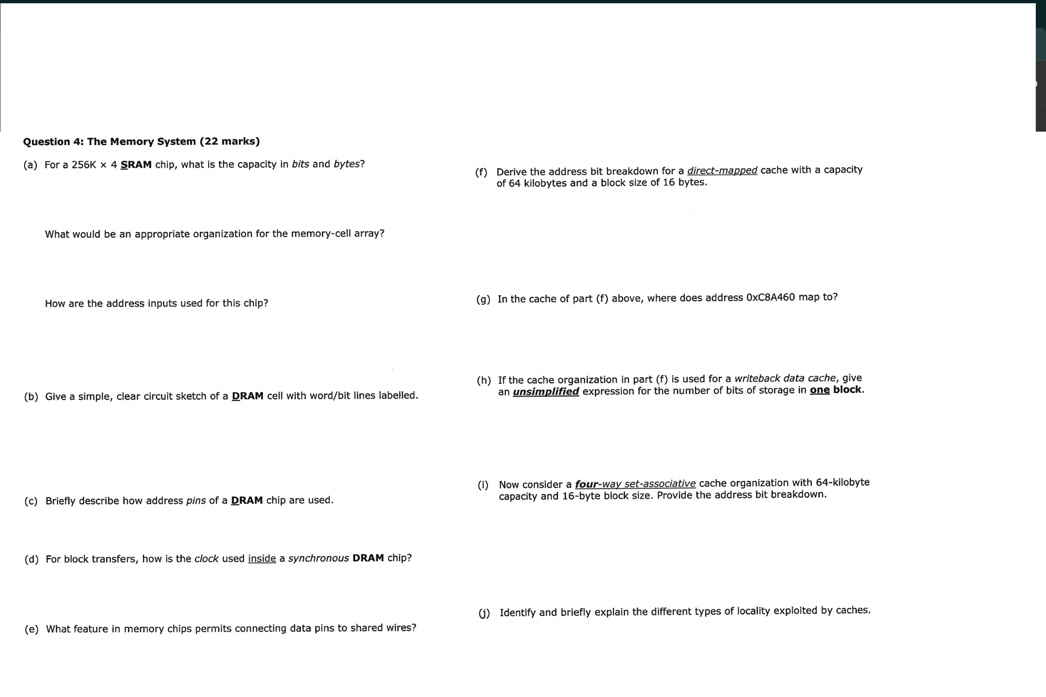
Question: executed. Write logic expressions for the control signals that are given below.Question 4 : The Memory System ( 2 2 marks ) ( a )
executed. Write logic expressions for the control signals that are given below.Question : The Memory System marks
a For a SRAM chip, what is the capacity in bits and bytes?
f Derive the address bit breakdown for a directmapped cache with a capacity
of kilobytes and a block size of bytes.
What would be an appropriate organization for the memorycell array?
How are the address inputs used for this chip?
b Give a simple, clear circuit sketch of a DRAM cell with wordbit lines labelled.
c Briefly describe how address pins of a DRAM chip are used.
d For block transfers, how is the clock used inside a synchronous DRAM chip?
e What feature in memory chips permits connecting data pins to shared wires?
g In the cache of part above, where does address xCA map to
h If the cache organization in part is used for a writeback data cache, give
an unsimplified expression for the number of bits of storage in one block.
i Now consider a fourway setassociative cache organization with kilobyte
capacity and byte block size. Provide the address bit breakdown.
j Identify and briefly explain the different types of locality exploited by caches.
IRen
MEMwrite
f The register file has two bit data outputs. Briefly identify all reg. file inputs.

Step by Step Solution
There are 3 Steps involved in it
1 Expert Approved Answer
Step: 1 Unlock


Question Has Been Solved by an Expert!
Get step-by-step solutions from verified subject matter experts
Step: 2 Unlock
Step: 3 Unlock


