

Question: Exercise 2: Design and test a simple logic circuit. A simple computer architecture with three instructions is described Figure 3.4 in the textbook: 0 opcode
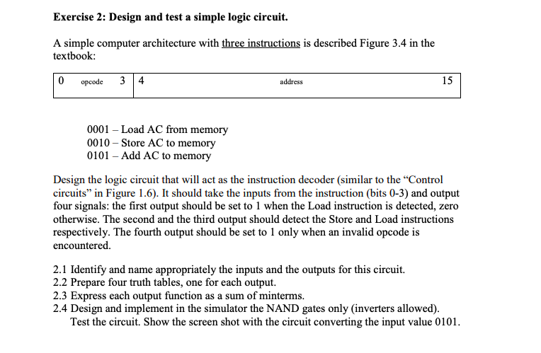
Exercise 2: Design and test a simple logic circuit. A simple computer architecture with three instructions is described Figure 3.4 in the textbook: 0 opcode 3 address address 15 0001 - Load AC from memory 0010 - Store AC to memory 0101 - Add AC to memory Design the logic circuit that will act as the instruction decoder (similar to the "Control circuits" in Figure 1.6). It should take the inputs from the instruction (bits 0-3) and output four signals: the first output should be set to 1 when the Load instruction is detected, zero otherwise. The second and the third output should detect the Store and Load instructions respectively. The fourth output should be set to 1 only when an invalid opcode is encountered 2.1 Identify and name appropriately the inputs and the outputs for this circuit. 2.2 Prepare four truth tables, one for each output. 2.3 Express each output function as a sum of minterms. 2.4 Design and implement in the simulator the NAND gates only (inverters allowed) Test the circuit. Show the screen shot with the circuit converting the input value 0101. Exercise 2: Design and test a simple logic circuit. A simple computer architecture with three instructions is described Figure 3.4 in the textbook: 0 opcode 3 address address 15 0001 - Load AC from memory 0010 - Store AC to memory 0101 - Add AC to memory Design the logic circuit that will act as the instruction decoder (similar to the "Control circuits" in Figure 1.6). It should take the inputs from the instruction (bits 0-3) and output four signals: the first output should be set to 1 when the Load instruction is detected, zero otherwise. The second and the third output should detect the Store and Load instructions respectively. The fourth output should be set to 1 only when an invalid opcode is encountered 2.1 Identify and name appropriately the inputs and the outputs for this circuit. 2.2 Prepare four truth tables, one for each output. 2.3 Express each output function as a sum of minterms. 2.4 Design and implement in the simulator the NAND gates only (inverters allowed) Test the circuit. Show the screen shot with the circuit converting the input value 0101
Step by Step Solution
There are 3 Steps involved in it

Get step-by-step solutions from verified subject matter experts