

Question: Exercise 2.1 Write RTL Verilog code to implement the design given in Figure 2.21. Generate the appropriate reset signal for the feedback register used in
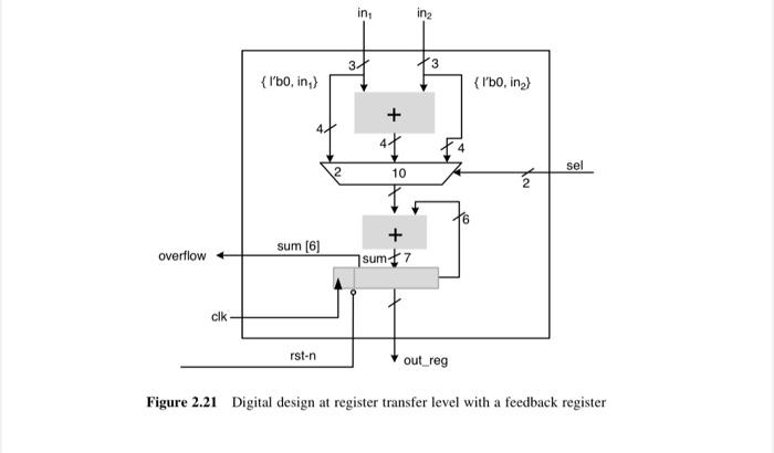
Exercise 2.1 Write RTL Verilog code to implement the design given in Figure 2.21. Generate the appropriate reset signal for the feedback register used in the design. Develop a test plan and write a stimulus to test the design for functional correctness. Also write a test case to count the number of cycles it takes for the register out reg to overflow for in1 and in 2 and sel set to 1. Also, code the design and stimulus in SystemVerilog. Figure 2.21 Digital design at register transfer level with a feedback register
Step by Step Solution
There are 3 Steps involved in it
1 Expert Approved Answer
Step: 1 Unlock

Question Has Been Solved by an Expert!
Get step-by-step solutions from verified subject matter experts
Step: 2 Unlock
Step: 3 Unlock