

Question: Write RTL Verilog code of the module device under test given in Figure 2.22. Four 8 bit inputs, in 1 , in 2,in3 and in
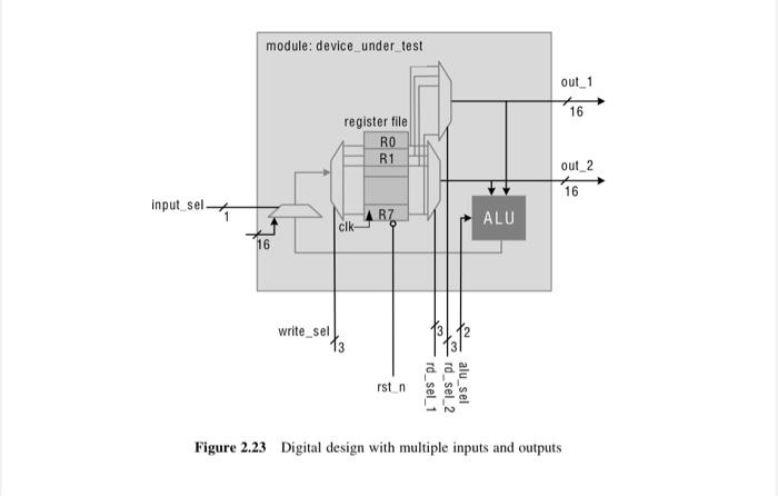
Write RTL Verilog code of the module device under test given in Figure 2.22. Four 8 bit inputs, in 1 , in 2,in3 and in 4 , are input to four 8 bit registers, RO, R1, R 2 and R3, respectively, at every positive edge of the clock. Four values in these registers are added, and bitwise AND operation is performed on the values stored in these registers to produce out 1 and out 2. Exercise 2.5 Write an RTL Verilog code and its stimulus to implement and test the module device under test given in Figure 2.23. The inputs and outputs of the module are shown. Generate a 20 time unit clock c1k from the stimulus, as werll as a rst n signal to reset the device before the first positive edge of the clock. The widths of each input and output signals are shown. Write test vectors by varying all the input signals in each test. Make sure each test vector is valid only for one clock period. Use the moni tor statement to print the values of the inputs and outputs on the screen. Finally, rewrite the stimulus in SystemVerilog and use coverage to test the design for selective ranges of input values. Use datapaths of exercise 2.2 for the ALU. Exercise 2.6 Design a datapath with three 8 bit accumulators. The first accumulator, acc1, adds a 4 bit input da ta in acc1 in every clock cycle. The second accumulator, acc2, adds the first accumulator in itself, and the third accumulator, acc3, adds the first and second accumulators in itself in every clock cycle. Each accumulator has an asynchronous reset. Draw the RTL level diagram and code the design in RTL Verilog. Figure 2.23 Digital design with multiple inputs and outputs
Step by Step Solution
There are 3 Steps involved in it

Get step-by-step solutions from verified subject matter experts