

Question: Experiment # 1 2 Design of Synchronous Counters Objectives: 1 . Learn step by step design of a synchronous counter from a given state
Experiment #
Design of Synchronous Counters
Objectives:
Learn step by step design of a synchronous counter from a given state diagram using JK Flip Flops.
Design a nonsequential counter from a given state diagram.
Introduction:
You will design and build a synchronous counter using JK Flip Flops. The desired states will be given, and you will be required to design the custom counter that meets the design specification. The required design process was explained in the weekly lecture.
Lab Report Requirements:
You must submit all work including state diagrams, nextstate table, transition table, Karnaugh maps, derived expressions, and schematic drawing, be sure to answer the conclusion question. All work should be provided on this lab syllabus. You are also required to submit your Logisim circ file so your instructor can run and test your circuit!
Part
Objective :
Given a state diagram, design a synchronous up counter. Follow the design steps outlined below in the procedure.
Materials Required:
Logisim Procedure :
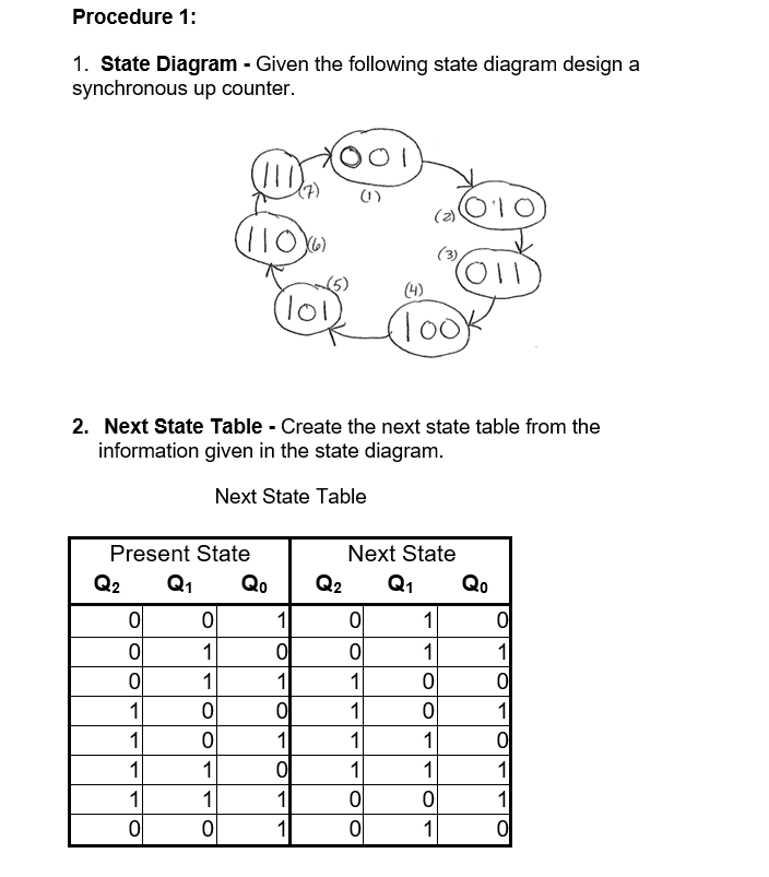
State Diagram Given the following state diagram design a synchronous up counter.
Next State Table Create the next state table from the information given in the state diagram.
Next State Table Procedure :
State Diagram Given the following state diagram design a synchronous up counter.
Next State Table Create the next state table from the information given in the state diagram.
Next State Table Procedure :
State Diagram Given the following state diagram design a synchronous up counter.
Next State Table Create the next state table from the information given in the state diagram.
Next State Table JK Flip Flop Transition Table Review the transition table for a JK Flip Flop given below. QN is the present state of the flip flop before a clock pulse and QN is the next state after a clock pulse The J and K input values are those that will cause the listed transition to occur. X is a "Don't Care" value, which could be a or a
Transition Table for a JK Flip Flop
begintabularccccc
hline multicolumnc Output Transitions & multicolumnc FlipFlip Inputs
mathrmQmathrmN & & mathrmQmathrmN & J & K
hline & square & & & X
hline & square & & & X
hline & square & & X &
hline & square & & X &
hline
endtabular Karnaugh Map Plot KMaps of the J and K inputs for each of the flipflops in the counter. Each cell in the KMap represents one of the present states in the counter sequence Refer to present state on NextState Table Remember to plot the "Don't Cares" also!
Group the s Group the s including as many "don't cares" as possible to maximize the simplification. Remember groups must include ldots cells. Groups must be indicated for credit. Write the expression Write the expression for the J and K inputs.
J
K
J
K
J
K
Implementation of Circuit Using the expressions found above draw an implementation of the counter using JK Flip Flops in Logisim Do NOT use Logisim Evolution! The expressions will define the connections to the J and K inputs of each JK FlipFlip used. Be sure to account for any other input asynchronous inputsenable if applicable Remember that you need to apply a clock input! You should connect an output pin to each Q output to monitor the operation of your circuit. When you draw your circuit be sure to arrange the Q output pins so they are presented with MSB on the left side and LSB on right side to make it easier to match your circuit outputs with the state machine diagram. You can review your work from Lab Latches and Flip Flops if you need to be reminded how to wire to a FlipFlop and simulate the circuit manually. RESULTS :
Test the counter Repeatedly apply a clock pulse manually you need to Tick twice to apply the full clock pulse! Compare your circuit Q output pins to each of the required states as given in the state diagram. The order of each state should match the order in the given state diagram. If the output states and the order in which they appear do not each match the design requirements, you need to go back and troubleshoot your design process to find the source of the error.
Conclusion :
Did your design perform the required function? Did the count outputs follow the given state diagram? Did any invalid counts appear? If so explain.
Step by Step Solution
There are 3 Steps involved in it
1 Expert Approved Answer
Step: 1 Unlock

Question Has Been Solved by an Expert!
Get step-by-step solutions from verified subject matter experts
Step: 2 Unlock
Step: 3 Unlock