

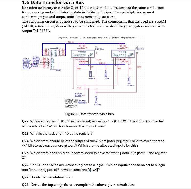
Question: Figure 1 : Data transfer via a bus Q 2 2 : Why are the pins 9 , 1 0 ( DE in the circuit
Figure : Data transfer via a bus
Q: Why are the pins DE in the circuit as well as O O in the circuit connected
with each other? Which functions do the inputs have?
Q: What is the task of pin at the register?
Q: Which state should be at the output of the bit register register or to avoid that the
bit storage saves a wrong word? Which are the allocated inputs for this?
Q: Which state does an output control need to have for storing data in register and register
Q: Can O and O be simultaneously set to a logic Which inputs need to be set to a logic
one for realizing part c In which state are
Q: Create the simulation table.
Q: Derive the input signals to accomplish the above given simulation.
Step by Step Solution
There are 3 Steps involved in it
1 Expert Approved Answer
Step: 1 Unlock

Question Has Been Solved by an Expert!
Get step-by-step solutions from verified subject matter experts
Step: 2 Unlock
Step: 3 Unlock