

Question: Figure 1.8 shows the conventional inverting amplifier configuration with a 10k? load resistor at the output. R1 Vin 1KQ NJ 741 0 Vout AWG1 10KQ
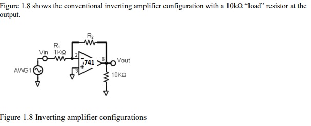
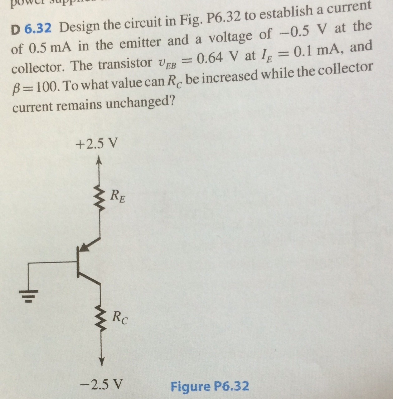
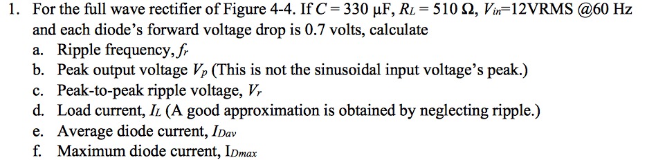
Figure 1.8 shows the conventional inverting amplifier configuration with a 10k? "load" resistor at the output. R1 Vin 1KQ NJ 741 0 Vout AWG1 10KQ Figure 1.8 Inverting amplifier configurationsD 6.32 Design the circuit in Fig. P6.32 to establish a current of 0.5 mA in the emitter and a voltage of -0.5 V at the collector. The transistor UEB = 0.64 V at IF = 0.1 mA, and B = 100. To what value can Re be increased while the collector current remains unchanged? +2.5 V RE RC -2.5 V Figure P6.321. For the full wave rectifier of Figure 4-4. If C= 330 UF, RL = 510 0, Vin=12VRMS @60 Hz and each diode's forward voltage drop is 0.7 volts, calculate a. Ripple frequency, fr b. Peak output voltage Vp (This is not the sinusoidal input voltage's peak.) c. Peak-to-peak ripple voltage, Vr d. Load current, IL (A good approximation is obtained by neglecting ripple.) e. Average diode current, IDav f. Maximum diode current, IDmax
Step by Step Solution
There are 3 Steps involved in it

Get step-by-step solutions from verified subject matter experts