

Question: Figure 4.9: design block diagram - Implement the Verilog code for circuit shown in Figure 4.9 page 38. (Write only the main Verilog code you
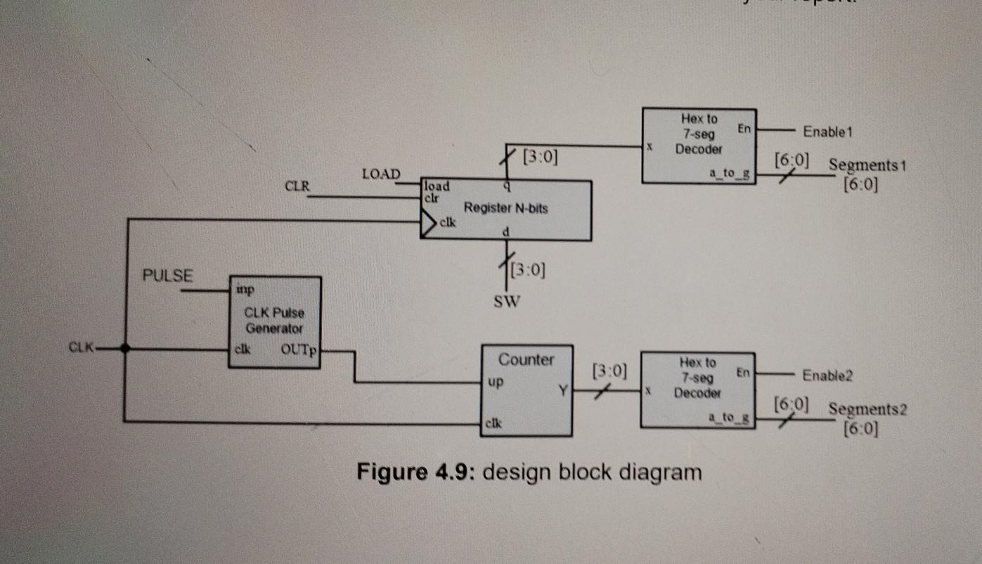
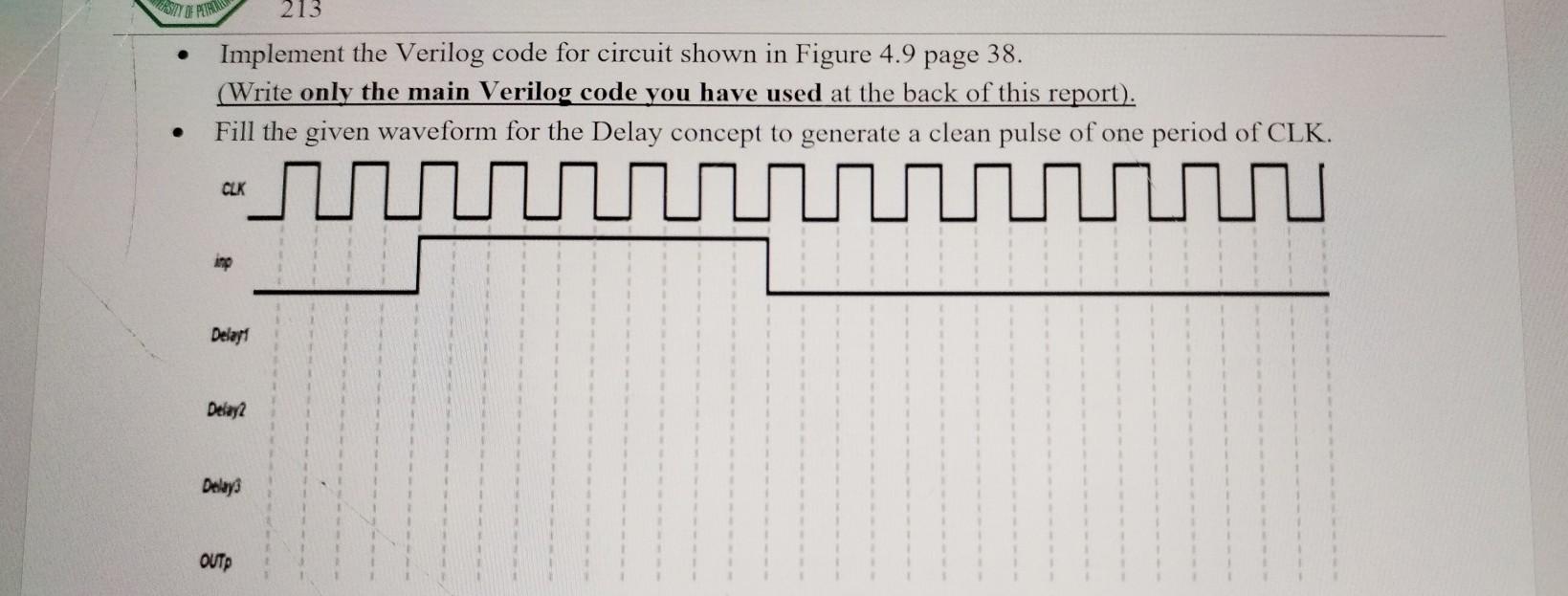
Figure 4.9: design block diagram - Implement the Verilog code for circuit shown in Figure 4.9 page 38. (Write only the main Verilog code you have used at the back of this report). - Fill the given waveform for the Delav concent to generate a clean pulse of one period of CLK
Step by Step Solution
There are 3 Steps involved in it
1 Expert Approved Answer
Step: 1 Unlock

Question Has Been Solved by an Expert!
Get step-by-step solutions from verified subject matter experts
Step: 2 Unlock
Step: 3 Unlock