

Question: Help Please help me finish the verilog and test bench simulation for the Clocked SR Flip-flop Clocked SR Flip-flop: A elocked SR flip-flop is created
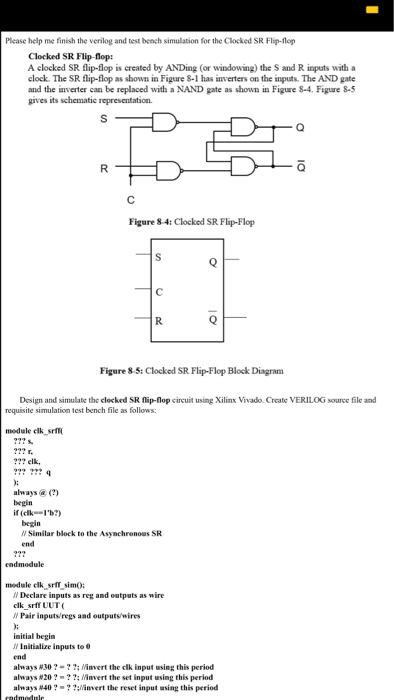
Please help me finish the verilog and test bench simulation for the Clocked SR Flip-flop Clocked SR Flip-flop: A elocked SR flip-flop is created by ANDing (or windowing) the S and R inputs with a clock. The SR flip-flop as shown in Figure 8-1 has inverters on the inputs. The AND gate and the inverter can be replaced with a NAND gate as shown in Figure 8-4. Figure 8-5 gives its schematic Figure 8 4: Clocked SR Flip-Flop Figure 8 5: Clocked SR Flip-Flop Block Diagram Design and simulate the clocked SR flip-lop circuit using Xilins Vivado. Create VERILOG source file and requisite simulation test bench file as follows: module elk srf 227s 222 r. 22 elk always@ (?) if (clk-1'b7) N Similar block to the Asynchronous SR end module clk srifT simo Declare inputs as reg and outputs as wire clk srff UUT Pair inputs/regs and outputs/wires initial begin Initialize inputs to end always #30-: Minvert the clk input using this period always #20 ?-??; /invert the set input using this period always#40 ?-? ?://invert the reset input usiag this period
Step by Step Solution
There are 3 Steps involved in it

Get step-by-step solutions from verified subject matter experts