

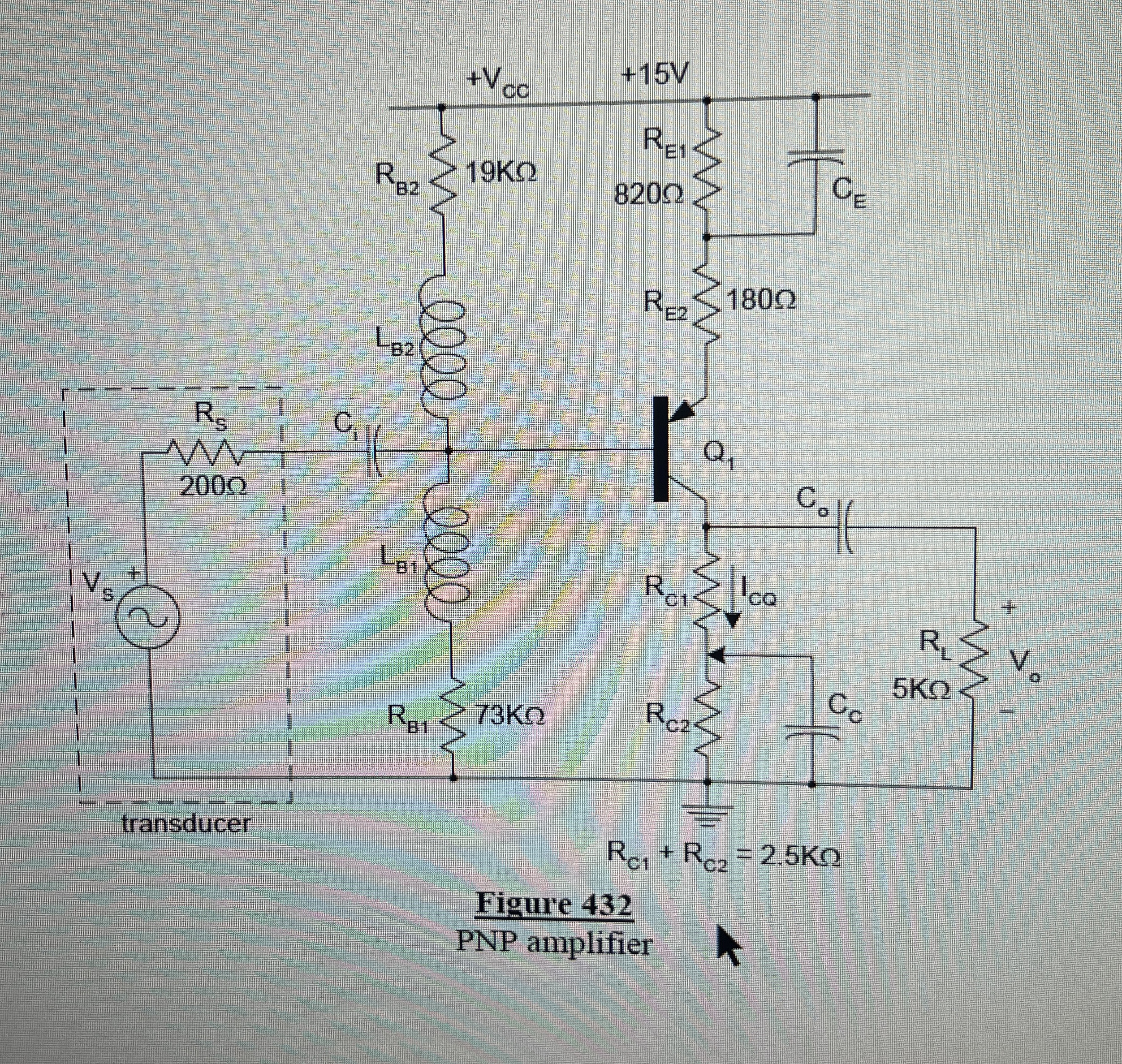
Question: Help please The schematic of a single - stage PNP BJT amplifier is shown in Figure 4 3 2 . The purpose of this amplifier
Help please
The schematic of a singlestage PNP BJT amplifier is shown in Figure The purpose of this amplifier is to process low frequency, upper midband signals from the transducer and to the load resistor The collector resistor is a trim pot with its center tap connected to the bypass capacitor Model parameters for are given below.
a Calculate the value for the dc collector current Ice.
b Calculate the range of the magnitude of smallsignal, midband transducer voltage gain resulting from the minimum and maximum values for That is calculate the range for determined by
c Calculate values for and to produce a magnitude of the transducer voltage gain of
As usual, the transducer voltage gain is
defined as
Step by Step Solution
There are 3 Steps involved in it
1 Expert Approved Answer
Step: 1 Unlock

Question Has Been Solved by an Expert!
Get step-by-step solutions from verified subject matter experts
Step: 2 Unlock
Step: 3 Unlock