

Question: Hi, please teach me with specific details answer for this question. Thank you. Figure Q7 shows the address decoding logic for a microprocessor system with
Hi, please teach me with specific details answer for this question. Thank you.
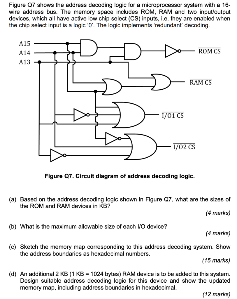
Figure Q7 shows the address decoding logic for a microprocessor system with a 16 wire address bus. The memory space includes ROM, RAM and two input/output devices, which all have active low chip select (CS) inputs, i.e. they are enabled when the chip select input is a logic ' 0 '. The logic implements 'redundant' decoding. Figure Q7. Circuit diagram of address decoding logic. (a) Based on the address decoding logic shown in Figure Q7, what are the sizes of the ROM and RAM devices in KB? (4 marks) (b) What is the maximum allowable size of each I/O device? (4 marks) (c) Sketch the memory map corresponding to this address decoding system. Show the address boundaries as hexadecimal numbers. (15 marks) (d) An additional 2KB ( 1KB=1024 bytes) RAM device is to be added to this system. Design suitable address decoding logic for this device and show the updated memory map, including address boundaries in hexadecimal. (12 marks)
Step by Step Solution
There are 3 Steps involved in it

Get step-by-step solutions from verified subject matter experts