

Question: Hints: For 5 . 5 , part b , in order for step 3 to be the bottleneck, you need to find a positive batch
Hints: For part b in order for step to be the bottleneck, you need to find a positive batch size such that under this batch size, step s capacity is no larger than Step s capacity, and step s capacity is also no larger than step capacity. If such a batch size does not exist, then it is not possible for step to be the bottleneck.QJCL Inc. JCL Inc. is a major chip manufacturing firm that sells its products to computer manufacturers like Dell, HP and others. In simplified terms, chip making at JCL Inc. involves three basic operations: depositing, patterning, and etching.
Depositing: Using chemical vapor deposition CVD technology, an insulating material is deposited on the wafer surface, forming a thin layer of solid material on the chip.
Patterning: Photolithography projects a microscopic circuit pattern on the wafer surface, which has a lightsensitive chemical like the emulsion on photographic film. It is repeated many times as each layer of the chip is built.
Etching: Etching removes selected material from the chip surface to create the device structures.
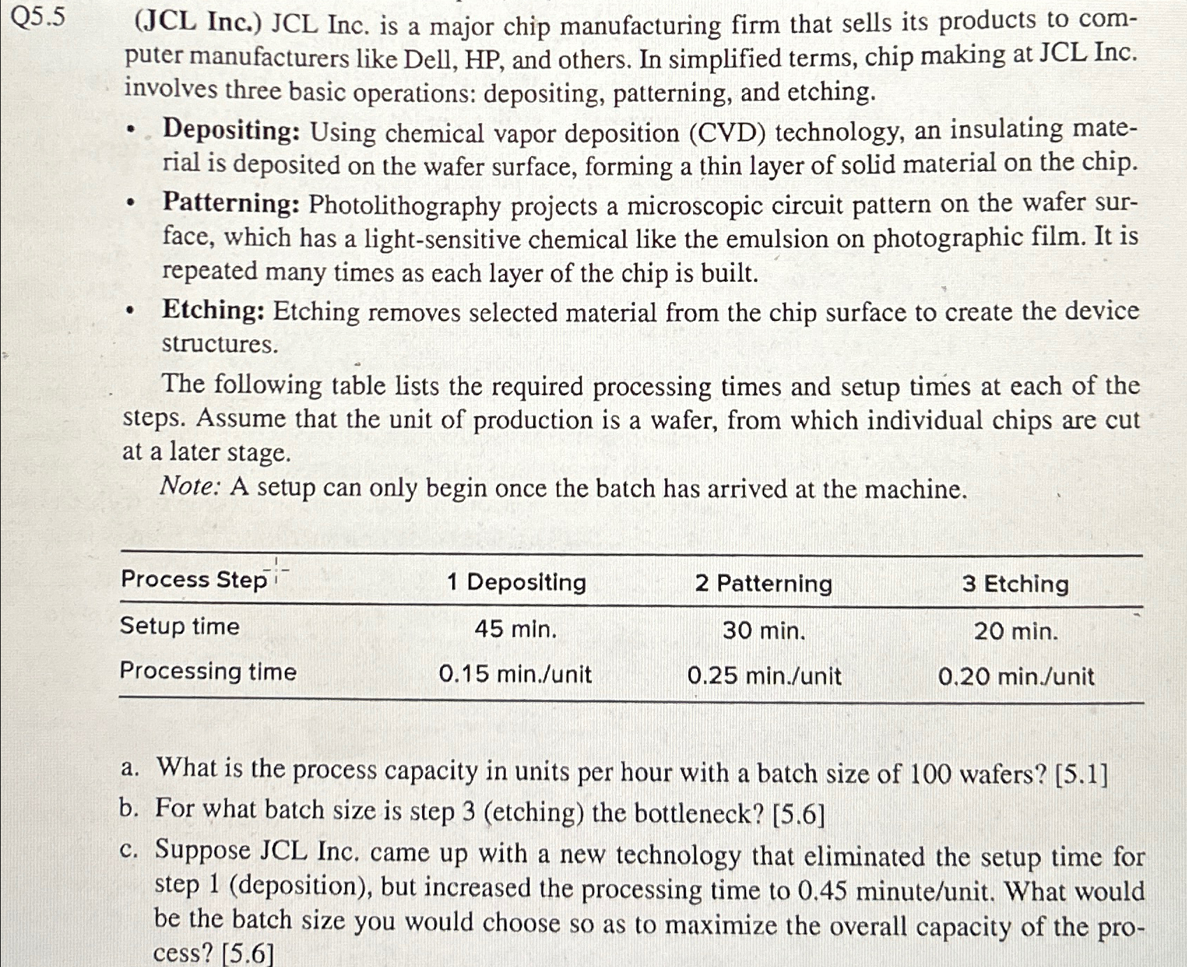
The following table lists the required processing times and setup times at each of the steps. Assume that the unit of production is a wafer, from which individual chips are cut at a later stage.
Note: A setup can only begin once the batch has arrived at the machine.
tableProcess Step Depositing, Patterning, EtchingSetup time,min.,min.,min.Processing time,minnit,minnit,nit
Step by Step Solution
There are 3 Steps involved in it
1 Expert Approved Answer
Step: 1 Unlock

Question Has Been Solved by an Expert!
Get step-by-step solutions from verified subject matter experts
Step: 2 Unlock
Step: 3 Unlock