

Question: How would I write the verilog for the FSM explained below? MO MI M2 Cin -Ft-1 SWI H CLK FSM RESET CLR W[2:0] CLK CLK
How would I write the verilog for the FSM explained below?
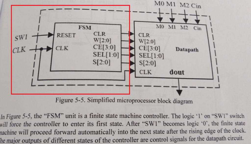
MO MI M2 Cin -Ft-1 SWI H CLK FSM RESET CLR W[2:0] CLK CLK CE[3:0] SEL[1:0] S[2:0] MO MI M2 Cin CLR W[2:0] CE[3:0] Datapath SEL[1:0] S[2:0] CLK dout -- -- - - - - - - - Figure 5-5. Simplified microprocessor block diagram In Figure 5-5, the FSM unit is a finite state machine controller. The logic '1' on SW1" switch will force the controller to enter its first state. After SW1 becomes logic '0', the finite state machine will proceed forward automatically into the next state after the rising edge of the clock. The major outputs of different states of the controller are control signals for the datapath circuit. MO MI M2 Cin -Ft-1 SWI H CLK FSM RESET CLR W[2:0] CLK CLK CE[3:0] SEL[1:0] S[2:0] MO MI M2 Cin CLR W[2:0] CE[3:0] Datapath SEL[1:0] S[2:0] CLK dout -- -- - - - - - - - Figure 5-5. Simplified microprocessor block diagram In Figure 5-5, the FSM unit is a finite state machine controller. The logic '1' on SW1" switch will force the controller to enter its first state. After SW1 becomes logic '0', the finite state machine will proceed forward automatically into the next state after the rising edge of the clock. The major outputs of different states of the controller are control signals for the datapath circuit
Step by Step Solution
There are 3 Steps involved in it

Get step-by-step solutions from verified subject matter experts