

Question: I need help fixing my portF registers so my C-PROGRAMMING code can work. It is a two push-button code for the TM4C123G LaunchPad. #include tm4c123gh6pm.h
I need help fixing my portF registers so my C-PROGRAMMING code can work. It is a two push-button code for the TM4C123G LaunchPad. 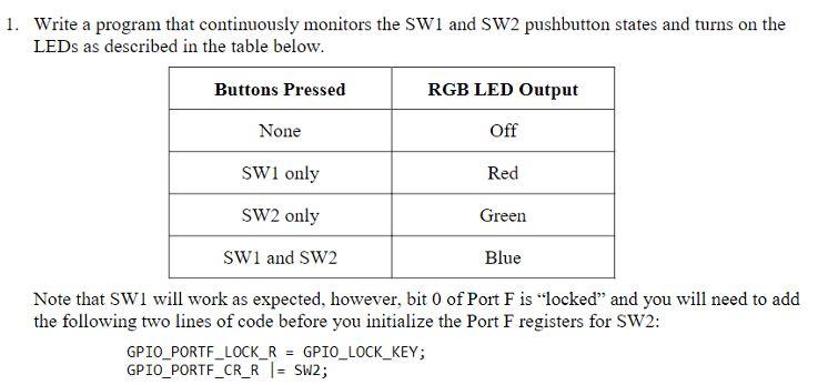
#include "tm4c123gh6pm.h" // device specific include file
#define BLUE BIT2//BIT 2 or 0x5 is blue, BIT1 or 0x3 is red, BIT3 or 0x8 is green, yellow is 0xA #define RED BIT1 #define GREEN BIT3 #define WHITE 0xE #define UNLOCK_CODE 0x4C4F4 #define SW1 BIT4 #define SW2 BIT0
int main(void) {
volatile int temp; // temporary variable to force peripheral bus read
// activate clock for GPIO Port F SYSCTL_RCGC2_R |= SYSCTL_RCGC2_GPIOF;
// allow a few cycles for clock to start temp = SYSCTL_RCGC2_R;
// unlock GPIO Port F & allow changes GPIO_PORTF_LOCK_R |= UNLOCK_CODE; GPIO_PORTF_CR_R |= SW2;
// enable Port F Bit 2 connected to white LED as digital output, For full colour spectrum GPIO_PORTF_DIR_R &= ~WHITE; GPIO_PORTF_DEN_R |= WHITE;
//Set Switch 1 & 2 as an input with a pull-up GPIO_PORTF_DIR_R &= ~SW1; GPIO_PORTF_PUR_R |= SW1; GPIO_PORTF_DEN_R |= SW1; GPIO_PORTF_DIR_R &= ~SW2; GPIO_PORTF_PUR_R |= SW2; GPIO_PORTF_DEN_R |= SW2;
while (1) { if(!(GPIO_PORTF_DATA_R & SW1) && (GPIO_PORTF_DATA_R & SW2)){
GPIO_PORTF_DATA_R |= RED; // toggle ON Red LED if button 1 is pressed } else(GPIO_PORTF_DATA_R &= ~RED); // toggle OFF Red LED if button 1 is not pressed
if(!(GPIO_PORTF_DATA_R & SW2) && (GPIO_PORTF_DATA_R & SW1)){
GPIO_PORTF_DATA_R |= GREEN; // toggle green LED toggle OFF Red LED if button 1 is not pressed } else(GPIO_PORTF_DATA_R &= ~GREEN);
if(!(GPIO_PORTF_DATA_R & (SW1 | SW2))){
GPIO_PORTF_DATA_R |= BLUE; // toggle ON Blue LED if button 1 & 2 is pressed } else(GPIO_PORTF_DATA_R &= ~BLUE); // toggle OFF Blue LED if button 1 & 2 is not pressed } }
 screenshot of registers from the circuit board
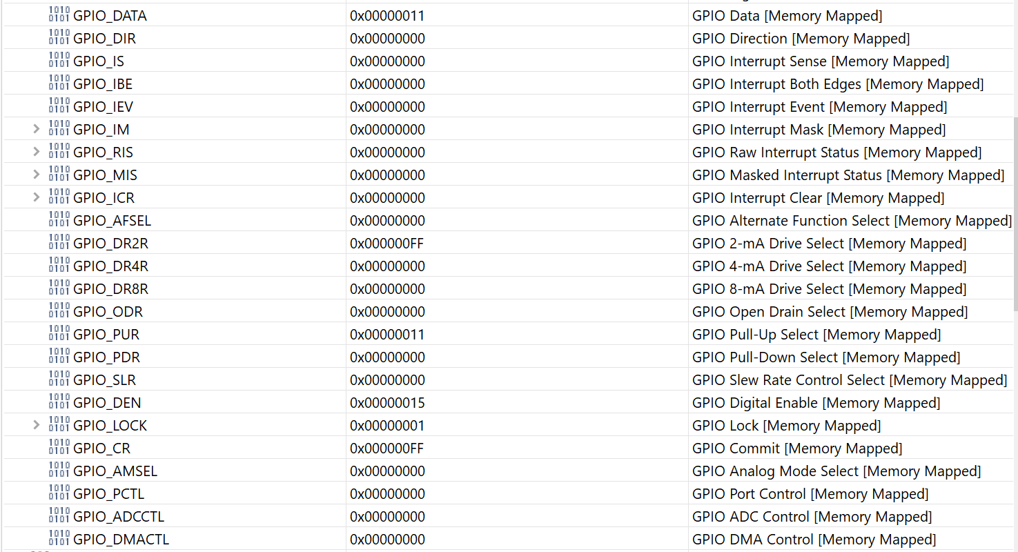
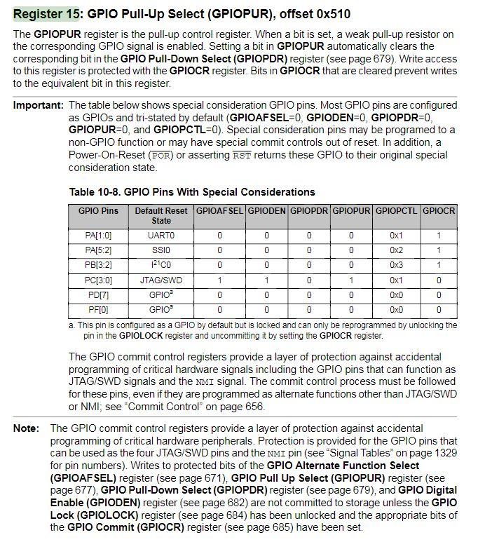
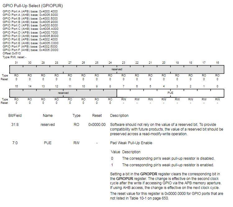
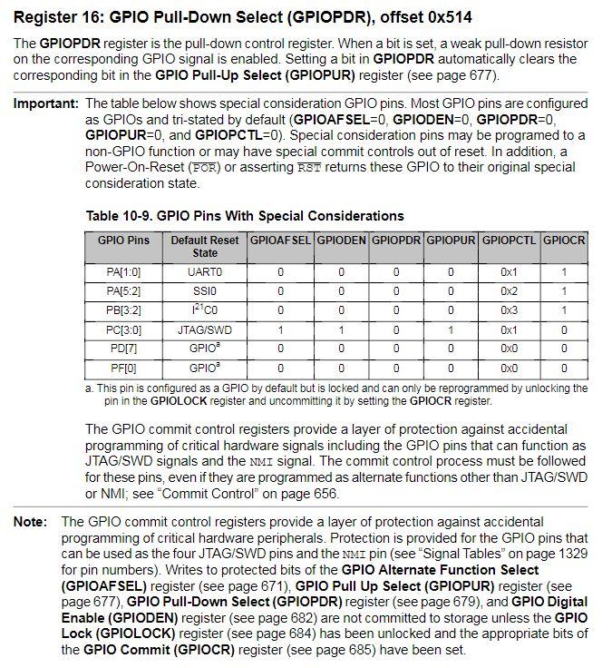
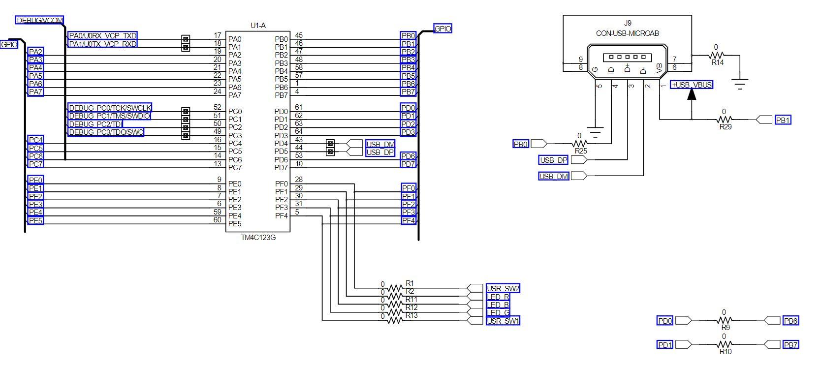
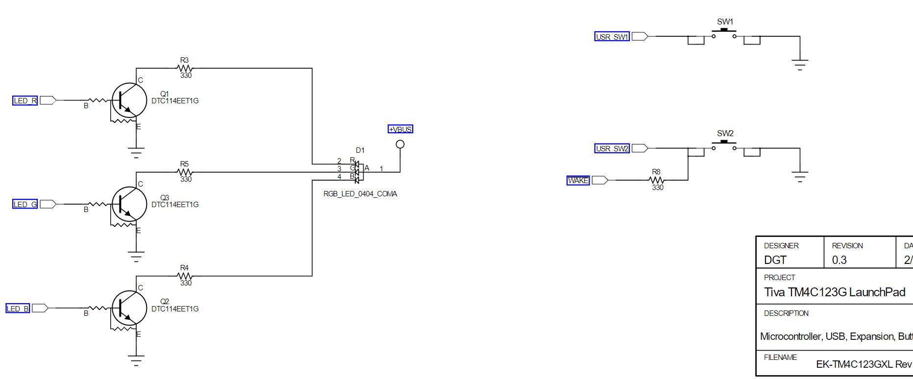
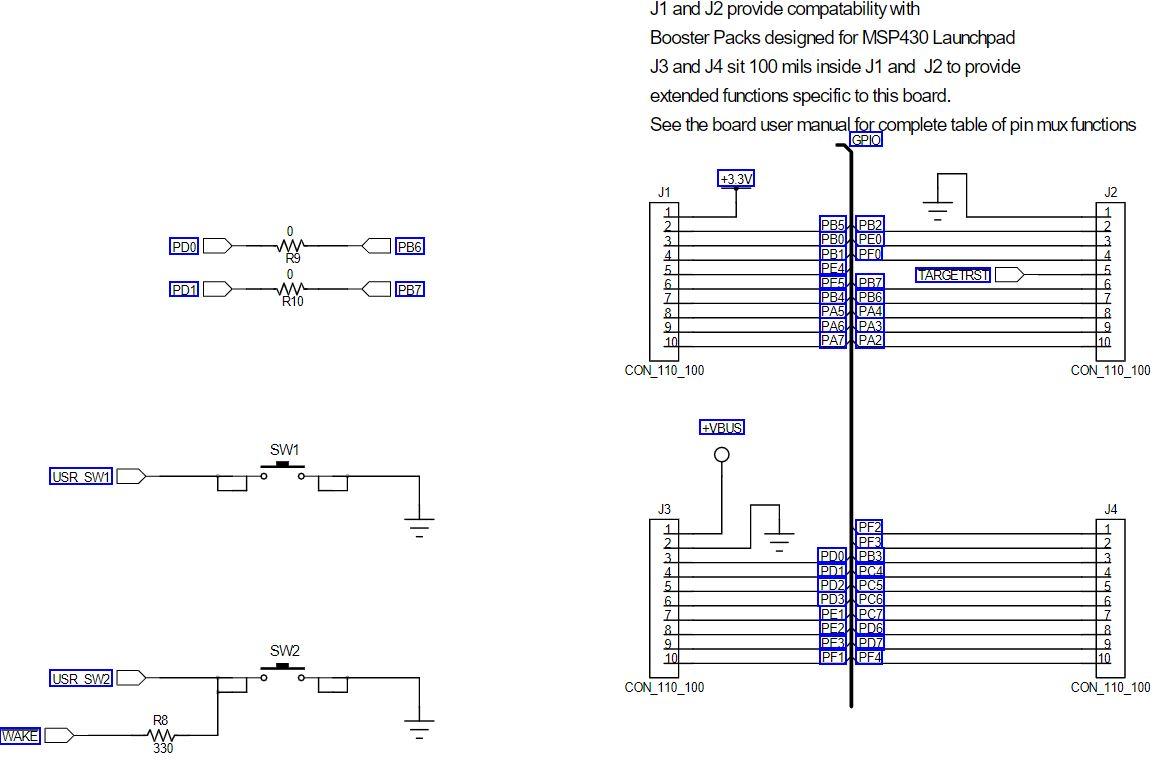
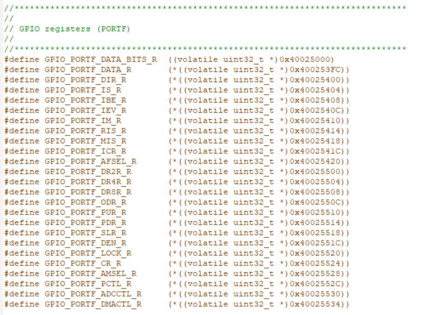
1. Write a program that continuously monitors the SW1 and SW2 pushbutton states and turns on the LEDs as described in the table below. Buttons Pressed RGB LED Output None Off SW1 only Red SW2 only Green SW1 and SW2 Blue Note that SWI will work as expected, however, bit 0 of Port F is "locked" and you will need to add the following two lines of code before you initialize the Port F registers for SW2: GPIO_PORTF_LOCK_R = GPIO_LOCK_KEY; GPIO_PORTF_CR_R I = SW2; // GPIO registers (PORTF) * //***** #define GPIO_PORTF_DATA_BITS_R ((volatile uint32_t * ) 0x40025000) #define GPIO PORTF_DATA_R (*((volatile uint32_t *) 0x400253FC)) #define GPIO_PORTF_DIR_R (*((volatile uint32_t *) 0x40025400)) #define GPIO_PORTF_IS_R (*((volatile uint32_t *) 0x40025404)) #define GPIO PORTF_IBE_R (*((volatile uint32_t *)0x40025408)) #define GPIO PORTF_IEV_R (*((volatile uint32_t *) 0x4002540C)) #define GPIO PORTF_IM_R (*((volatile uint32_t *) 0x40025410)) #define GPIO_PORTF_RIS_R (* ((volatile uint32_t *) 0x40025414)) #define GPIO_PORTF_MIS_R (*((volatile uint32_t *) 0x40025418)) #define GPIO_PORTF_ICR_R (*((volatile uint32_t *) 0x40025410)) #define GPIO PORTF AFSEL R (*((volatile uint32_t *) 0x40025420) ) #define GPIO_PORTF_DR2R_R (* ((volatile uint32_t *) 0x40025500)) #define GPIO_PORTF_DR4R_R (*((volatile uint32_t *) 0x40025504)) #define GPIO_PORTF_DRSR_R (*((volatile uint32_t *)0x40025508)) #define GPIO_PORTF_ODR_R (*((volatile uint32_t *) 0x4002550C)) #define GPIO_PORTF_PUR_R (* ((volatile uint32_t *)0x40025510)) #define GPIO PORTF_PDR_R (* ((volatile uint32_t *) 0x40025514) ) #define GPIO_PORTF_SLR_R (* ((volatile uint32_t *)0x40025518)) #define GPIO PORTF_DEN R (*((volatile uint32_t *) 0x4002551C)) #define GPIO_PORTF_LOCK_R (* ((volatile uint32_t *)0x40025520)) #define GPIO PORTF_CR_R (*((volatile uint32_t *) 0x40025524)) #define GPIO_PORTF_AMSEL_R (* ((volatile uint32_t *)0x40025528)) #define GPIO PORTF_PCTL_R (*((volatile uint32_t *) 0x4002552C)) #define GPIO_PORTF_ADCCTL_R (*((volatile uint32_t *) 0x40025530)) #define GPIO PORTF_DMACTL_R (* ((volatile uint32_t *) 0x40025534) ) Ox00000011 Ox00000000 Ox00000000 Ox00000000 Ox00000000 Ox00000000 Ox00000000 Ox00000000 Ox00000000 Ox00000000 Ox000000FF Ox00000000 1010 BOLIGPIO_DATA DILA GPIO_DIR 0101 bibi GPIO_IS 1010 bibi GPIO_IBE 1010 Dibi GPIO_IEV 1010 > didi GPIO_IM 1010 > Dibi GPIO_RIS 1010 > Dibi GPIO_MIS 1010 > Dibi GPIO_ICR bibi GPIO_AFSEL 1019 bibi GPIO_DR2R DOBA GPIO_DR4R DODA GPIO_DRER BADA GPIO ODR 0101 DADA GPIO_PUR Dibi GPIO_PDR 1010 1010 dibi GPIO_SLR 1010 Dibi GPIO_DEN 1010 > Dibi GPIO_LOCK 1010 DIO GPIO_CR 1010 Dibi GPIO_AMSEL dibi GPIO_PCTL Dibi GPIO_ADCCTL 1010 DIDA GPIO_DMACTL GPIO Data (Memory Mapped] GPIO Direction [Memory Mapped] GPIO Interrupt Sense [Memory Mapped] GPIO Interrupt Both Edges [Memory Mapped] GPIO Interrupt Event [Memory Mapped] GPIO Interrupt Mask [Memory Mapped] GPIO Raw Interrupt Status [Memory Mapped] GPIO Masked Interrupt Status [Memory Mapped] GPIO Interrupt Clear [Memory Mapped] GPIO Alternate Function Select [Memory Mapped] GPIO 2-mA Drive Select [Memory Mapped] GPIO 4-mA Drive Select [Memory Mapped] GPIO 8-mA Drive Select [Memory Mapped] GPIO Open Drain Select [Memory Mapped] GPIO Pull-Up Select [Memory Mapped] GPIO Pull-Down Select [Memory Mapped] GPIO Slew Rate Control Select [Memory Mapped] GPIO Digital Enable [Memory Mapped] GPIO Lock [Memory Mapped] GPIO Commit [Memory Mapped] GPIO Analog Mode Select [Memory Mapped] GPIO Port Control [Memory Mapped] GPIO ADC Control [Memory Mapped] GPIO DMA Control [Memory Mapped] Ox00000000 Ox00000000 Ox00000011 Ox00000000 Ox00000000 Ox00000015 Ox00000001 Ox000000FF Ox00000000 Ox00000000 Ox00000000 Ox00000000 Register 15: GPIO Pull-Up Select (GPIOPUR), offset 0x510 The GPIOPUR register is the pull-up control register. When a bit is set, a weak pull-up resistor on the corresponding GPIO signal is enabled. Setting a bit in GPIOPUR automatically clears the corresponding bit in the GPIO Pull-Down Select (GPIOPDR) register (see page 679). Write access to this register is protected with the GPIOCR register. Bits in GPIOCR that are cleared prevent writes to the equivalent bit in this register. Important: The table below shows special consideration GPIO pins. Most GPIO pins are configured as GPIOs and tri-stated by default (GPIOAF SEL=0, GPIODEN=0, GPIOPDR=0, GPIOPUR=0, and GPIOPCTL=0). Special consideration pins may be programed to a non-GPIO function or may have special commit controls out of reset. In addition, a Power-On-Reset (POR) or asserting RST returns these GPIO to their original special consideration state. 1 0 0 0 1 0 1 1 0 Table 10-8. GPIO Pins With Special Considerations GPIO Pins Default Reset GPIOAFSEL GPIODEN GPIOPDR GPIOPUR GPIOPCTL GPIOCR State PA[1:01 UARTO 0 0 0 0 Ox1 PA[5:2] SSIO 0 Ox2 PB[3:2] 12100 0 0 0 Ox3 PC(3:0) JTAG/SWD 1 0 1 Ox1 0 PD[7] GPIO 0 0 0 0 0 PF[O] GPIO 0 0 0 0 a. This pin is configured as a GPIO by default but is locked and can only be reprogrammed by unlocking the pin in the GPIOLOCK register and uncommitting it by setting the GPIOCR register. The GPIO commit control registers provide a layer of protection against accidental programming of critical hardware signals including the GPIO pins that can function as JTAG/SWD signals and the NMI signal. The commit control process must be followed for these pins, even if they are programmed as alternate functions other than JTAG/SWD or NMI; see "Commit Control" on page 656. Note: The GPIO commit control registers provide a layer of protection against accidental programming of critical hardware peripherals. Protection is provided for the GPIO pins that can be used as the four JTAG/SWD pins and the NMI pin (see "Signal Tables" on page 1329 for pin numbers). Writes to protected bits of the GPIO Alternate Function Select (GPIOAFSEL) register (see page 671), GPIO Pull Up Select (GPIOPUR) register (see page 677), GPIO Pull-Down Select (GPIOPDR) register (see page 679), and GPIO Digital Enable (GPIODEN) register (see page 682) are not committed to storage unless the GPIO Lock (GPIOLOCK) register (see page 684) has been unlocked and the appropriate bits of the GPIO Commit (GPIOCR) register (see page 685) have been set. GPIO Pull-Up Select (GPIOPUR) GPIO Port A (APB) base: 0x4000.4000 GPIO Port A (AHB) base: 0x4005.8000 GPIO Port B (APB) base: 0x4000.5000 GPIO Port B (AHB) base: 0x40059000 GPIO Port C (APB) base: 0x4000.0000 GPIO Port C (AHB) base: 0x4005.A000 GPIO Port D (APB) base: 0x4000.7000 GPIO Port D (AHB) base: 0x4005.8000 GPIO Port E (APB) base: 0x4002.4000 GPIO Port E (AHB) base: 0x4005.0000 GPIO Port F (APB) base: 0x4002.5000 GPIO Port F (AHB) base: 0x4005.DODO Offset Ox510 Type RW, reset - 31 30 29 28 27 28 25 24 23 22 21 20 19 18 17 18 1 T reserved 9 12 19 RO RO 0 Type Reset RO RO 0 RO 0 RO 0 RO 0 RO RO 0 RO leo RO 0 oo RO 0 RO 0 RO 0 RO 0 RO 0 o . . 0 0 . 15 14 13 12 11 10 9 8 7 B 5 4 4 3 2 1 1 0 reserved PUE RW RO RW RW RW RW RW lo a RW Type Reset RO 0 RW RO 0 RO 0 RO 0 RO 0 RO 0 RO D . . . - Bit/Field Name Type 31:8 reserved RO 7:0 PUE RW Reset Description 0x0000.00 Software should not rely on the value of a reserved bit. To provide compatibility with future products, the value of a reserved bit should be preserved across a read-modify-write operation. Pad Weak Pull-Up Enable Value Description The corresponding pin's weak pull-up resistor is disabled. The corresponding pin's weak pull-up resistor is enabled. Setting a bit in the GPIOPDR register clears the corresponding bit in the GPIOPUR register. The change is effective on the second clock cycle after the write if accessing GPIO via the APB memory aperture. If using AHB access, the change is effective on the next clock cycle. The reset value for this register is 0x0000.0000 for GPIO ports that are not listed in Table 10-1 on page 650. 0 1 Register 16: GPIO Pull-Down Select (GPIOPDR), offset 0x514 The GPIOPDR register is the pull-down control register. When a bit is set, a weak pull-down resistor on the corresponding GPIO signal is enabled. Setting a bit in GPIOPDR automatically clears the corresponding bit in the GPIO Pull-Up Select (GPIOPUR) register (see page 677). Important: The table below shows special consideration GPIO pins. Most GPIO pins are configured as GPIOs and tri-stated by default (GPIOAFSEL=0, GPIODEN=0, GPIOPDR=0, GPIOPUR=0, and GPIOPCTL=0). Special consideration pins may be programed to a non-GPIO function or may have special commit controls out of reset. In addition, a Power-On-Reset (POR) or asserting RST returns these GPIO to their original special consideration state. 1 0 0 0 1 1 Table 10-9. GPIO Pins With Special Considerations GPIO Pins Default Reset GPIOAFSEL GPIODEN GPIOPDR GPIOPUR GPIOPCTL GPIOCR State PA[1:01 UARTO 0 0 0 0 Ox1 PA[5:21 SSIO 0 Ox2 PB[3:2] 12.CO 0 0 0 0 0x3 1 PC[3:01 JTAG/SWD 1 0 1 Ox1 0 PD[7] GPIO 0 0 0 0 0 PF[0] GPIO 0 0 0 0 Oxo 0 a. This pin is configured as a GPIO by default but is locked and can only be reprogrammed by unlocking the pin in the GPIOLOCK register and uncommitting it by setting the GPIOCR register. The GPIO commit control registers provide a layer of protection against accidental programming of critical hardware signals including the GPIO pins that can function as JTAG/SWD signals and the NMI signal. The commit control process must be followed for these pins, even if they are programmed as alternate functions other than JTAG/SWD or NMl; see "Commit Control" on page 656. Note: The GPIO commit control registers provide a layer of protection against accidental programming of critical hardware peripherals. Protection is provided for the GPIO pins that can be used as the four JTAG/SWD pins and the NMI pin (see "Signal Tables" on page 1329 for pin numbers). Writes to protected bits of the GPIO Alternate Function Select (GPIOAFSEL) register (see page 671), GPIO Pull Up Select (GPIOPUR) register (see page 677), GPIO Pull-Down Select (GPIOPDR) register (see page 679), and GPIO Digital Enable (GPIODEN) register (see page 682) are not committed to storage unless the GPIO Lock (GPIOLOCK) register (see page 684) has been unlocked and the appropriate bits of the GPIO Commit (GPIOCR) register (see page 685) have been set. DEBUGNCOM U1-A GPIO J9 CON-USB-MICROAB PAO/UORX VCP TXD PAMUOTX VCP RXD GPIC PBO! PB1 PB2 | PBS 45 PBO PB1 46 47 PB2 48 PB3 PB4 58 PB5 57 DOOOO 9 8 7 6 PA2 PA3 PA4 PA5 PA6 PAZ w R14 PB4! 20 PA4 PB5 PB6H PB6! LO - +USB.VBUS PB7 17 PAO 18 19 PA1 PA2 20 21 22 23 PA5 24 PAS PAT 52 51 PCO 50 PC1 49 PC3 16 PC4 15 PC5 14 PC6 13 PC7 DEBUG PCO/TCK/SWCLK DEBUG PC1/TMS/SWDIO DEBUG PC2UDI DEBUG PC3/TDOSWOI B PD1 62 0 w R29 PB1 20 PC2 PB7 61 PDO PD2 63 64 PD3 PD4 PD5 53 PD6 PD7 10 PDO) PD1) PD2! PD3 USB DM USB DP PD6 PD7 PC4 PC5 PC6 PCA P w R25 USB DP USB DM 9 PEO PE1 PE2 PE3 PE4 PE5 PEO PE1 PE2 PE3 PE4 PE5 PFO PF1 PF2 PF3 PF4 28 29 30 31 5 PFO! PF1 PF2 PF3 PE4 59 60 TM4C123G w w R11 USR SW2 LED R LED B LED C USR SW1 R12 W R13 PDO 0 w R9 0 PB6 nn PD1 PB7 R10 SW1 USR SW1 R3 330 LED R Q1 DTC114EET1G B +VBUS SW2 USR SW2 D1 2 3 . R5 w 330 1 WAKE R8 w 330 RGB_LED_0404_COMA LED G Q3 DTC114EET1G DA DESIGNER DGT REVISION 0.3 2 R4 w PROJECT Tiva TM4C123G LaunchPad LED B Q2 DTC114EET1G DESCRIPTION Microcontroller, USB, Expansion, Buti FILENAME EK-TM4C123GXL Rev J1 and J2 provide compatability with Booster Packs designed for MSP430 Launchpad J3 and J4 sit 100 mils inside J1 and J2 to provide extended functions specific to this board. See the board user manual for complete table of pin mux functions GPIO +3.3V J2 PDO PB6 W R9 0 W- R10 J1 1 2 3 4 4 5 6 7 7 8 9 101 TARGETRST PD1 PB7 PB5PB2 PBOX PEOL PB11PFO PE PE5PB7 IPB4 IPB6 PA5U PA4 PAZ PAZ 10 CON_110_100 CON_110_100 VBUS SW1 USR SW1 J3 J4 = 1 1 2 3 4 5 6 7 8 PF2 PF3 PDO PB3 PDI!!PCA PD11 PD2!!PCS , PD3U!PCG PE14. PC7 PE2|PDG PEWPD7 PF1 PF4 SW2 10. 10 USR SW21 O CON_110_100 CON_110_100 R8 W 330 TH WAKE
Step by Step Solution
There are 3 Steps involved in it

Get step-by-step solutions from verified subject matter experts