

Question: I need the code and testbench for the given design with an elaborate explanationof an instruction and its operand. The meaning of the syntax Rxlarr
I need the code and testbench for the given design with an elaborate explanationof an instruction and its operand. The meaning of the syntax Rxlarr is that the contents of register are
loaded into register RX The mv move instruction allows data to be copied from one register to another. For
the mvi move immediate instruction the expression RxlarrD indicates that the bit constant is loaded into
register
Table Instructions performed in the processor.
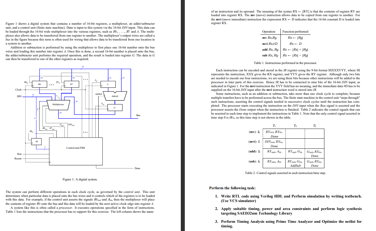
Each instruction can be encoded and stored in the IR register using the bit format IIIXXXYYY, where III
represents the instruction, XXX gives the RX register, and YYY gives the RY register. Although only two bits
are needed to encode our four instructions, we are using three bits because other instructions will be added to the
processor in later parts of this exercise. Hence has to be connected to nine bits of the bit DIN input, as
indicated in Figure For the mvi instruction the YYY field has no meaning, and the immediate data # has to be
supplied on the bit DIN input after the mvi instruction word is stored into
Some instructions, such as an addition or subtraction, take more than one clock cycle to complete, because
multiple transfers have to be performed across the bus. The finite state machine in the control unit "steps through"
such instructions, asserting the control signals needed in successive clock cycles until the instruction has com
pleted. The processor starts executing the instruction on the DIN input when the Run signal is asserted and the
processor asserts the Done output when the instruction is finished. Table indicates the control signals that can
be asserted in each time step to implement the instructions in Table Note that the only control signal asserted in
time step is in so this time step is not shown in the table.
Table Control signals asserted in each instructiontime step.
Perform the following task:
Write RTL code using Verilog HDL and Perform simulation by writing testbench.
Use VCS simulator
Apply suitable timing, power and area constraints and perform logic synthesis
targeting SAEDnm Technology Library
Perform Timing Analysis using Prime Time Analyzer and Optimize the netlist for
timing.
Step by Step Solution
There are 3 Steps involved in it
1 Expert Approved Answer
Step: 1 Unlock

Question Has Been Solved by an Expert!
Get step-by-step solutions from verified subject matter experts
Step: 2 Unlock
Step: 3 Unlock