

Question: I need Verilog code in Modelsim for the Task attached here in the picture. Also write the test code (TESTBENCH) for testing the code that
I need Verilog code in Modelsim for the Task attached here in the picture. Also write the test code (TESTBENCH) for testing the code that you right. Please don't send me incomplete and errorred code at all. Also plz write the code according to all the required parameters.
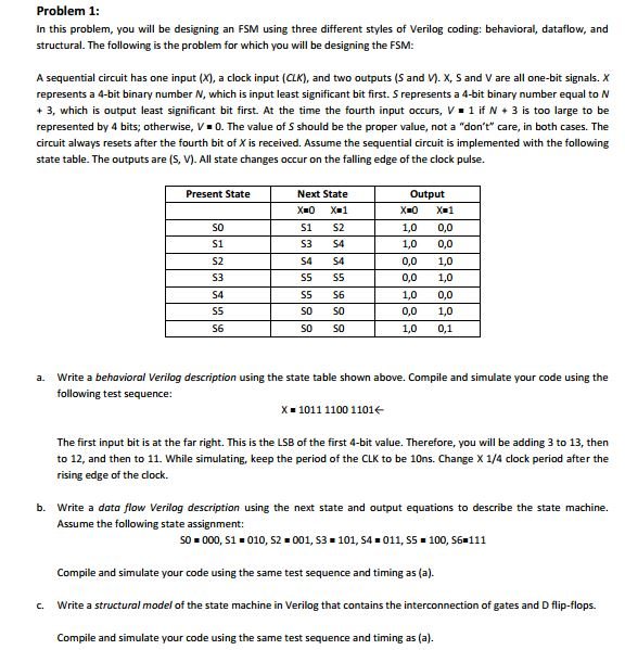
Problem 1 In this problem, you will be designing an FSM using three different styles of Verilog coding: behavioral, dataflow, and structural. The following is the problem for which you will be designing the FSMM A sequential circuit has one input (X, a clock input (CLK), and two outputs (S and V). X, S and V are all one-bit signals.X represents a 4-bit binary number N, which is input least significant bit first. S represents a 4-bit binary number equal to N + 3, which is output least significant bit first. At the time the fourth input occurs, V-1 if N + 3 is too large to be represented by 4 bits, otherwise, V0. The value of S should be the proper value, not a "dont" care, in both cases. The circuit always resets after the fourth bit of X is received. Assume the sequential circuit is implemented with the following state table. The outputs are (S, V). All state changes occur on the falling edge of the clock pulse. Present State Next State Output SO S1 S2 S3 S4 S1 S2 S3 S4 S4 S4 1,0 0,0 1,0 0,0 0,0 1,0 0,0 1,0 1,0 0,0 0,0 1,0 1,0 0,1 SS S6 SO SO SO SO S6 Write a behavioral Verilog description using the state table shown above. Compile and simulate your code using the following test sequence: a. X 1011 1100 1101 The first input bit is at the far right. This is the LSB of the first 4-bit value. Therefore, you will be adding 3 to 13, then to 12, and then to 11. While simulating, keep the period of the CLK to be 10ns. Change X 1/4 clock period after the rising edge of the clock. b. Write a data flow Verilog description using the next state and output equations to describe the state machine. Assume the following state assignment: SO 000, S1 010, S2 001, S3 101, S4 011, SS 100, s6 111 Compile and simulate your code using the same test sequence and timing as (a). Write a structural model of the state machine in Verilog that contains the interconnection of gates and D flip-flops. Compile and simulate your code using the same test sequence and timing as (a). c. Problem 1 In this problem, you will be designing an FSM using three different styles of Verilog coding: behavioral, dataflow, and structural. The following is the problem for which you will be designing the FSMM A sequential circuit has one input (X, a clock input (CLK), and two outputs (S and V). X, S and V are all one-bit signals.X represents a 4-bit binary number N, which is input least significant bit first. S represents a 4-bit binary number equal to N + 3, which is output least significant bit first. At the time the fourth input occurs, V-1 if N + 3 is too large to be represented by 4 bits, otherwise, V0. The value of S should be the proper value, not a "dont" care, in both cases. The circuit always resets after the fourth bit of X is received. Assume the sequential circuit is implemented with the following state table. The outputs are (S, V). All state changes occur on the falling edge of the clock pulse. Present State Next State Output SO S1 S2 S3 S4 S1 S2 S3 S4 S4 S4 1,0 0,0 1,0 0,0 0,0 1,0 0,0 1,0 1,0 0,0 0,0 1,0 1,0 0,1 SS S6 SO SO SO SO S6 Write a behavioral Verilog description using the state table shown above. Compile and simulate your code using the following test sequence: a. X 1011 1100 1101 The first input bit is at the far right. This is the LSB of the first 4-bit value. Therefore, you will be adding 3 to 13, then to 12, and then to 11. While simulating, keep the period of the CLK to be 10ns. Change X 1/4 clock period after the rising edge of the clock. b. Write a data flow Verilog description using the next state and output equations to describe the state machine. Assume the following state assignment: SO 000, S1 010, S2 001, S3 101, S4 011, SS 100, s6 111 Compile and simulate your code using the same test sequence and timing as (a). Write a structural model of the state machine in Verilog that contains the interconnection of gates and D flip-flops. Compile and simulate your code using the same test sequence and timing as (a). c
Step by Step Solution
There are 3 Steps involved in it

Get step-by-step solutions from verified subject matter experts