

Question: Implement the following combinational logic circuit in VHDL using Quartus. Provide a printout of the code. At the very top of your code, include a
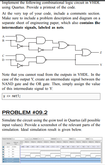
Implement the following combinational logic circuit in VHDL using Quartus. Provide a printout of the code. At the very top of your code, include a comments section, Make sure to include a problem description and diagram on a separate sheet of engineering paper, which also contains the intermediate signals, labeled as nets. Do Note that you cannot read from the outputs in VHDL. In the case of the output Y, create an intermediate signal between the NAND gate and the OR gate. Then, simply assign the value of this intermediate signal to Y y netl; PROBLEM #09.2 Simulate the circuit using the gsim tool in Quartus (all possible input values). Provide a screenshot of the relevant parts of the simulation. Ideal simulation result is given below
Step by Step Solution
There are 3 Steps involved in it

Get step-by-step solutions from verified subject matter experts