

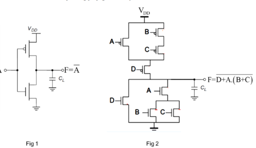
Question: Implement the inverter shown in Fig 1 using 1 8 - nm FinFET GPDK ( a ) using Cadence Simulate the inverter using transient analysis
Implement the inverter shown in Fig using nm FinFET GPDK
a using Cadence Simulate the inverter using transient analysis for a load capacitance of CL fF Present waveforms at the input A and at the output F Select the size of the transistors so that tpHL tpLH Extract the values of the propagation delays from the waveforms.
b using Cadence Implement the circuit in Fig and size the transistors in a way that the longest propagation delays for the lowtohigh and the hightolow transitions match with that of the inverter. i Present the output waveform when A B C D and A B C D and extract the corresponding propagation delays.
Step by Step Solution
There are 3 Steps involved in it
1 Expert Approved Answer
Step: 1 Unlock

Question Has Been Solved by an Expert!
Get step-by-step solutions from verified subject matter experts
Step: 2 Unlock
Step: 3 Unlock