

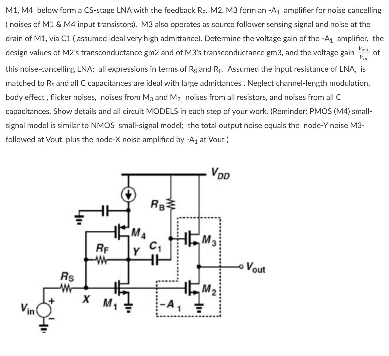
Question: M 1 , M 4 below form a CS - stage LNA with the feedback R F . M 2 , M 3 form an
M M below form a CSstage LNA with the feedback form an amplifier for noise cancelling noises of M & M input transistors M also operates as source follower sensing signal and noise at the drain of M via C assumed ideal very high admittance Determine the voltage gain of the amplifier, the design values of Ms transconductance gm and of Ms transconductance gm and the voltage gain of this noisecancelling LNA; all expressions in terms of and Assumed the input resistance of LNA, is matched to and all capacitances are ideal with large admittances. Neglect channellength modulation, body effect, flicker noises, noises from and noises from all resistors, and noises from all capacitances. Show details and all circuit MODELS in each step of your work. Reminder: PMOS M smallsignal model is similar to NMOS smallsignal model; the total output noise equals the nodeY noise Mfollowed at Vout, plus the node X noise amplified by at Vout
Step by Step Solution
There are 3 Steps involved in it
1 Expert Approved Answer
Step: 1 Unlock

Question Has Been Solved by an Expert!
Get step-by-step solutions from verified subject matter experts
Step: 2 Unlock
Step: 3 Unlock