

Question: Make the solution clear and simple, please Consider the circuit below that adds the two 2-bit numbers A1A0 and B1B0. The delay of each gate
Make the solution clear and simple, please
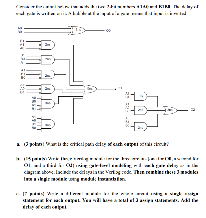
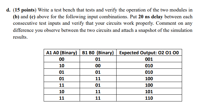
Consider the circuit below that adds the two 2-bit numbers A1A0 and B1B0. The delay of each gate is written on it. A bubble at the input of a gate means that input is inverted: BO 3ns B1 A1 2ns B1 BO 2ns A1 A1 B1 BO. 2ns A1 2ns B1 5ns 01 A1 B1 Ins BO A1- B1 3ns A1 BO 2ns 3ns 02 A1 B1 BO B1 3ns BO 2ns a. (3 points) What is the critical path delay of each output of this circuit? b. (15 points) Write three Verilog module for the three circuits (one for 00, a second for 01, and a third for 02) using gate-level modeling with each gate delay as in the diagram above. Include the delays in the Verilog code. Then combine these 3 modules into a single module using module instantiation. c. (7 points) Write a different module for the whole circuit using a single assign statement for each output. You will have a total of 3 assign statements. Add the delay of each output. d. (15 points) Write a test bench that tests and verify the operation of the two modules in (b) and (c) above for the following input combinations. Put 20 ns delay between each consecutive test inputs and verify that your circuits work properly. Comment on any difference you observe between the two circuits and attach a snapshot of the simulation results. 00 01 A1 A0 (Binary) B1 BO (Binary) Expected Output: 02 01 00 001 10 00 010 01 01 010 01 100 11 01 100 101 11 11 110 11 10 11
Step by Step Solution
There are 3 Steps involved in it

Get step-by-step solutions from verified subject matter experts