

Question: MAKE THS WTH MULTSM PROGRAM PLEASE Description and The Design Work Let us start with Figure 1 which shows a digital computer system that contains
MAKE THS WTH MULTSM PROGRAM PLEASE
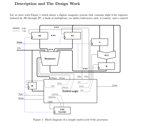
Description and The Design Work Let us start with Figure 1 which shows a digital computer system that contains eight 8-bit registers indexed by RD through R7, a bank of multiplexer, an adder/subtractor unit, a counter, and a control RO R7 Clock DIN ALU Mulliplexers IR Done Ron R7 Rout... Rout Ain Bout IR Asen DINO Control Logic Bn ISBN MSBE Clear Reset 2-bit Counter Figure 1: Block dingram of a simple multi-cycle 8-bit processor a unit Data is input in this system via the hit DIN input this data wide thrugh DIN input can be loaded through the 8-bit wide multiplexer unit into the various registers, such as RO.....R7 and A. The multiplexer should also allow data to be transferred from one register to another. In this digital system, the wires can carry 1-bit information except if its drawn bold which would mean that it is a bus that can carry 8-bits of information in parallel In case of addition or subtraction operations, the multiplexer first places one 8-bit mumber onto the bus wires and load this number into register A. At the next clock edge, a second 8-bit number is placed onto the bus and therefore the adder/subtracter unit executes the required operation, and the result can finally be loaded into register B (upon an enable signal for that register to store the appropriate value). Finally, in the next clock edge, the data in register B is transferred to one of the other registers as required. As can be understood, the digital system can perform different operations in each clock cycle, mainly governed by the control signals of the control logic. This unit determines when is a particular data placed onto the bus and also which of the registers should be loaded with the data. For instance, if the control unit asserts the signals Ryout and Ain (which gives logical "l"), then the multiplexer will place the contents of register RT onto the bus and this data will be automatically loaded by the next active clock edge (could be positive or negative) into register A. The set of executable operations are specified in the form of instructions. Table 1 lists the instructions that the CPU is intended to support for this project. The left column shows the name of an instruc tion and its operand/s. We use indexes y E {0,1,2,3,4,5,6,7} to indicate one of the registers. When the contents of register Ry are koaded into register Rx, we use a syntax Rx + Ry). Hence, the Table 1: The instructions of the procesor OP code Operation and Operandis Executed Function TER 01 mi Rr, REED 10 adres NUDEL 11 sub R, Hy HERE - Table 2: The set of control signals asserted for each instruction and time step. Instruction Type Th T Ririn, Ryout I Rin Done Rrin, DINO I Rin Done Ririn, Bout. add I Rin Rout Ryout Done Bin, Ririn, Ryout, Boul sub I Rin Rout Asen Done Ain, 2.1 (30pts) Draw the datapath and corresponding registers/counters and ALU as shown in Figure 1. You are more than welcome to use your pervious ALU design Lab 2) in your cirenit. 2.2 (20pts) Design the control logie unit in Figure 1 by drawing the appropriate truth tables and performing simplifications. In order to ease your work, we provided Table 3, at the end of the docu ment for you to fill in. 2.3 (Bonus +5pts) As an additional step, you may like to add the overflow and carry out outputs of the ALU as two additional inputs for the Control unit while making decisions. 4 Demonstration In this project, you are going to have to demonstrate your operational CPU in our prearranged session in order to get full credit. In demonstration session, for automating the following instruction execution and data processing, it might be advisable to use a RAM, kad it with the appropriate set of data (both instructions as well as data) and use the counter to jump to the appropriate location to load information on DIN input of the CPU. Although this is not required, it can certainly expedite your project demonstration. I recom- mend you look at built-in RAM capabilities of Multisim and get yourself familiar with it. mwi R5, 0xB8 R5 + OxBS, mw R6, RS6 +25] (2) mwi R5,0x6F R5 - Oxtil, (3) adel R6, R5 R6 - 16+ (RS), aded R5, R5 R5 R5+ (RS), (5) sub R5 R6 RS - R5 R6] (6) 3.2 (10pts) What are the contents of Rs and Rs at the end of executing above instructions? Use hex displays and LEDs to demonstrate the functionality, 3.3 (10pts) We do not have a special instruction to execute other operations that may come handy However, it might be possible to execute those operations using multiple registers and the available instruction types. Please generate the appropriate instructions to perform the following steps and comment on the function we are trying to make our CPU execute. Suppose we have three registers Ra, Rb and Re. We would like to manipulate the contents of Rb and transfer it to Ra. RbOxIF Re-Rol Re-Re-R Ra-Ro-Re Ra Ra - 1 What's the final content of register Rb? How many cock cycles it takes to execute this operation? Note that it would have been much more convenient to add this new instruction to our ISA to run the corresponding operation faster
Step by Step Solution
There are 3 Steps involved in it

Get step-by-step solutions from verified subject matter experts