

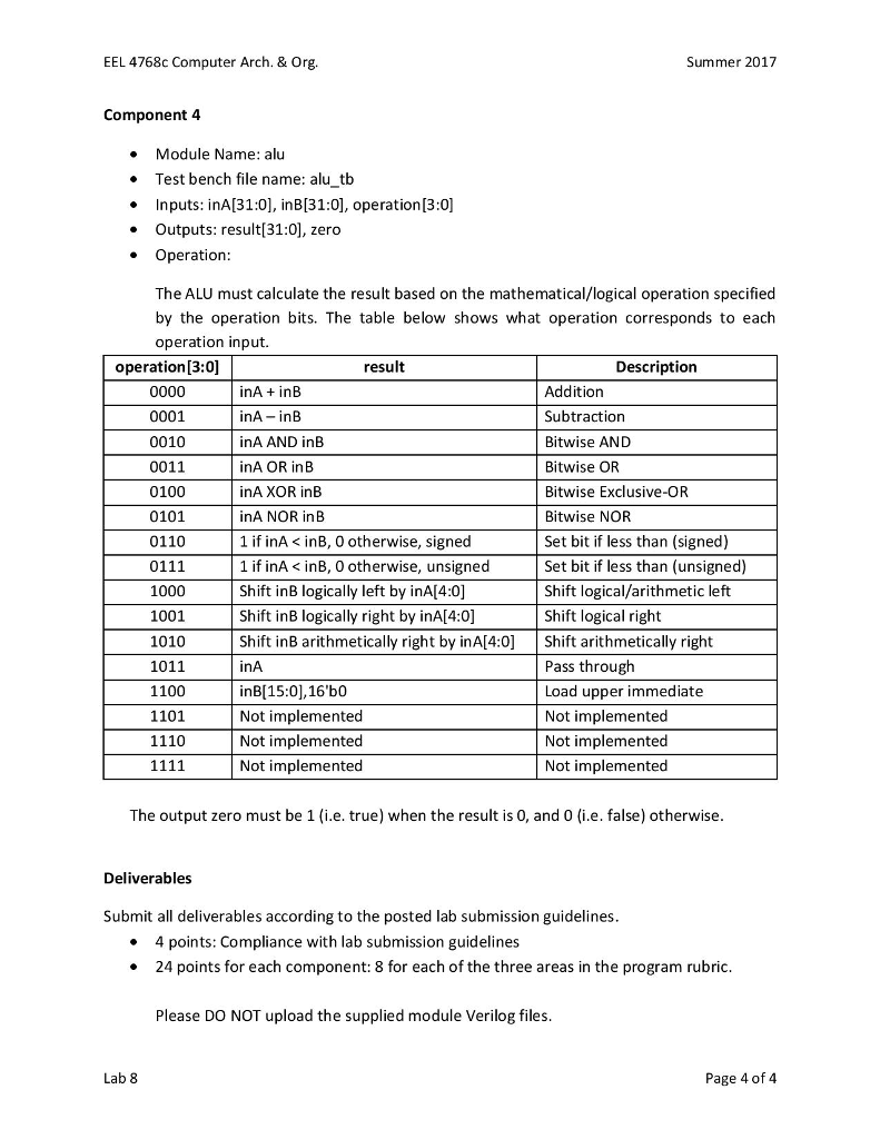
Question: // Module name: alu_a // Version 1.1 // Module Desc: ALU for single-cycle 32-bit RISC system // Inputs: inA - One 32-bit operand input //
// Module name: alu_a
// Version 1.1
// Module Desc: ALU for single-cycle 32-bit RISC system
// Inputs: inA - One 32-bit operand input
// inB - Second 32-bit operand input
// operation - 4-bit alu operation, see alu_ops.txt for listing
// Outputs: result - 32-bit calculated result based on inputs and operation
// zero - set to 1 when the result is 0, used for branching
// Internal parameters:
// alu_ops.txt provides alphanumeric names for 4-bit operations
module alu(
input [31:0] inA,
input [31:0] inB,
input [3:0] operation,
output [31:0] result,
output zero
);
`include "alu_ops.txt" // provides parameters for more readable operations
wire [31:0] inA, inB;
wire [3:0] operation;
wire zero;
reg [31:0] result;
always @ (inA or inB or operation)
begin
case(operation)
OP_ADD: result = inA+inB;
OP_SUB: result = inA-inB;
OP_AND: result = inA & inB;
OP_OR : result = inA | inB;
OP_XOR: result = inA ^ inB;
OP_NOR: result = inA ~| inB;
OP_SLT: result = ($signed(inA)
OP_SLTU: result = (inA OP_SLL: result = inB OP_SRL: result = inB >> inA[4:0]; OP_SRA: result = $signed(inB) >>> inA[4:0]; OP_INA: result = inA; OP_LUI: result = {inB[15:0],16'b0}; OP_NOP1: result = inA; OP_NOP2: result = inA; OP_NOP3: result = inA; endcase end assign zero = (result == 32'b0)?1:0; endmodule // Module name: alu_b // Version 1.1 // Module Desc: ALU for single-cycle 32-bit RISC system // Inputs: inA - One 32-bit operand input // inB - Second 32-bit operand input // operation - 4-bit alu operation, see alu_ops.txt for listing // Outputs: result - 32-bit calculated result based on inputs and operation // zero - set to 1 when the result is 0, used for branching // Internal parameters: // alu_ops.txt provides alphanumeric names for 4-bit operations module alu( input [31:0] inA, input [31:0] inB, input [3:0] operation, output [31:0] result, output zero ); `include "alu_ops.txt" // provides parameters for more readable operations wire [31:0] inA, inB; wire [3:0] operation; wire zero; reg [31:0] result; always @ (inA or inB or operation) begin case(operation) OP_ADD: result = inA+inB; OP_SUB: result = inA-inB; OP_AND: result = inA & inB; OP_OR : result = inA | inB; OP_XOR: result = inA ^ inB; OP_NOR: result = inA ~^ inB; OP_SLT: result = (inA OP_SLTU: result = (inA OP_SLL: result = inB OP_SRL: result = inB >> inA[4:0]; OP_SRA: result = $signed(inB) >> inA[4:0]; OP_INA: result = inA; OP_LUI: result = {inB[15:0],16'b0}; OP_NOP1: result = inA; OP_NOP2: result = inA; OP_NOP3: result = inA; endcase end assign zero = (result == 32'b0)?1:0; endmodule alu_ops.txt // ALU operations for alu.v and controlunit.v // Version 1.0 // data inputs are inA[31:0] and inB[31:0], 4 bit operation select // data output is result[31:0], zero = 1 if result==32'b0 parameter OP_ADD = 4'b0000; // inA + inB parameter OP_SUB = 4'b0001; // inA - inB parameter OP_AND = 4'b0010; // bitwise inA AND inB parameter OP_OR = 4'b0011; // bitwise inA OR inB parameter OP_XOR = 4'b0100; // bitwise inA XOR inB parameter OP_NOR = 4'b0101; // bitwise inA NOR inB parameter OP_SLT = 4'b0110; // if inA parameter OP_SLTU = 4'b0111; // if inA parameter OP_SLL = 4'b1000; // shift inB logical left by inA bits parameter OP_SRL = 4'b1001; // shift inB logical right by inA bits parameter OP_SRA = 4'b1010; // shift inB arithmetically right by inA bits parameter OP_INA = 4'b1011; // pass inA unchanged parameter OP_LUI = 4'b1100; // result is {inB[15:0],16'b0} parameter OP_NOP1 = 4'b1101; // not yet implemented parameter OP_NOP2 = 4'b1110; // not yet implemented parameter OP_NOP3 = 4'b1111; // not yet implemented // Module name: datamem_a // Module Desc: data memory for single-cycle 32-bit RISC system // Inputs: address - 32-bit address // datain - // WE - // clk - // writebyte - // writehalfword - // Outputs: data - 32-bit data located at memory address specified by addr, provided asynchronously // Internal parameters: // STARTADDR - 32-bit starting address for the memory // LENGTH - number of bytes in the memory // Notes: As RISC instruction memory, only addresses evenly divisible by 4 are expected. The module // will truncate the lower to bits and only provide instructions that are aligned. module datamem( address, // 32-bit memory address datain, // 32-bit memory contents WE, // Write enable clk, // clock, positive transition causes data write when WE = 1 writebyte, // write only a byte writehalfword, // write only a halfword data // 32-bit output ); parameter STARTADDR = 32'h1000_0000; parameter LENGTH = 32'h0000_1000; input [31:0] address, datain; input WE, clk, writebyte, writehalfword; output [31:0] data; wire [31:0] address, datain; wire [31:0] data; wire WE, clk, writebyte, writehalfword; reg [7:0] memory[STARTADDR:STARTADDR+LENGTH -1]; assign data = {memory[address],memory[address+1],memory[address+2],memory[address+3]}; // truncate so that address is 4-byte aligned always @(posedge clk) begin if (WE === 1) begin if (writebyte === 1) begin memory[address] = datain[7:0]; end else if (writehalfword === 1) begin {memory[address],memory[address+1]} = datain[15:0]; end else begin {memory[address],memory[address+1],memory[address+2],memory[address+3]} = datain; end end end endmodule // Module name: datamem_b // Module Desc: data memory for single-cycle 32-bit RISC system // Inputs: address - 32-bit address // datain - // WE - // clk - // writebyte - // writehalfword - // Outputs: data - 32-bit data located at memory address specified by addr, provided asynchronously // Internal parameters: // STARTADDR - 32-bit starting address for the memory // LENGTH - number of bytes in the memory // Notes: As RISC instruction memory, only addresses evenly divisible by 4 are expected. The module // will truncate the lower to bits and only provide instructions that are aligned. module datamem( address, // 32-bit memory address datain, // 32-bit memory contents WE, // Write enable clk, // clock, positive transition causes data write when WE = 1 writebyte, // write only a byte writehalfword, // write only a halfword data // 32-bit output ); parameter STARTADDR = 32'h1000_0000; parameter LENGTH = 32'h0000_1000; input [31:0] address, datain; input WE, clk, writebyte, writehalfword; output [31:0] data; wire [31:0] address, datain; wire [31:0] data; wire WE, clk, writebyte, writehalfword; reg [7:0] memory[STARTADDR:STARTADDR+LENGTH -1]; assign data = {memory[address+3],memory[address+2],memory[address+1],memory[address]}; // truncate so that address is 4-byte aligned always @(posedge clk) begin if (WE === 1) begin if (writebyte === 1) begin memory[address] = datain[7:0]; end else if (writehalfword === 1) begin {memory[address+1],memory[address]} = datain[15:0]; end else begin {memory[address+3],memory[address+2],memory[address+1],memory[address]} = datain; end end end endmodule // Module name: instmem_a // Module Desc: instruction memory for single-cycle 32-bit RISC system // Inputs: addr - 32-bit address // Outputs: data - 32-bit data located at memory address specified by addr, provided asynchronously // Internal parameters: // STARTADDR - 32-bit starting address for the memory // LENGTH - number of bytes in the memory // Notes: As RISC instruction memory, only addresses evenly divisible by 4 are expected. The module // will truncate the lower to bits and only provide instructions that are aligned. module instmem( addr, // 32-bit memory address data // 32-bit memory contents ); parameter STARTADDR = 32'h0040_0000; parameter LENGTH = 32'h0000_1000; // in bytes input [31:0] addr; output [31:0] data; wire [31:0] addr; wire [31:0] data; reg [7:0] memory[STARTADDR:STARTADDR+LENGTH -1]; // instruction stored as little endian assign data = {memory[{addr[31:2],2'b00}],memory[{addr[31:2],2'b01}],memory[{addr[31:2],2'b10}],memory[{addr[31:2],2'b11}]}; endmodule // Module name: instmem_b // Module Desc: instruction memory for single-cycle 32-bit RISC system // Inputs: addr - 32-bit address // Outputs: data - 32-bit data located at memory address specified by addr, provided asynchronously // Internal parameters: // STARTADDR - 32-bit starting address for the memory // LENGTH - number of bytes in the memory // Notes: As RISC instruction memory, only addresses evenly divisible by 4 are expected. The module // will truncate the lower to bits and only provide instructions that are aligned. module instmem( addr, // 32-bit memory address data // 32-bit memory contents ); parameter STARTADDR = 32'h0040_0000; parameter LENGTH = 32'h0000_1000; // in bytes input [31:0] addr; output [31:0] data; wire [31:0] addr; wire [31:0] data; // Note that since the memory is accessed in groups of 4-bytes, the address is internally divided by 4. reg [7:0] memory[STARTADDR:STARTADDR+LENGTH -1]; // instruction stored as little endian assign data = {memory[{addr[31:2],2'b11}],memory[{addr[31:2],2'b10}],memory[{addr[31:2],2'b01}],memory[{addr[31:2],2'b00}]}; endmodule // Module name: instmem_tb_ex // Module Desc: test bench for module instmem // Internal parameters: // STARTADDR - 32-bit starting address for the memory, must correspond to UUT // LENGTH - number of bytes in the memory, must correspond to UUT // // module instmem_tb_ex; parameter STARTADDR = 32'h0040_0000; parameter LENGTH = 32'h0000_1000; reg [31:0] addr; wire[31:0] data; reg [63:0] testvectors[0:100]; // array of test vector inputs reg [10:0] errors; // counts errors between UUT and TV known output reg [10:0] vectornum; // loop counter for processing the test vactors reg [31:0] i; // loop counter to initialize inst memory // Demonstrates a loop for initializing the first 100 location to specific values initial begin for (i=0; i uut.memory[STARTADDR+i] = i%256; // can only store 0-255 in a byte $display("Address: %h Contents: %h", STARTADDR+i, uut.memory[STARTADDR+i]); end end instmem #(STARTADDR, LENGTH) uut( .addr (addr), .data (data) ); endmodule // Module name: regfile_a // Module Desc: 32 32-bit registers for RISC processor // two asynchronous read ports, one synchronous write port // Inputs: // input1 - 5 bit index for read port 1 // input2 - 5 bit index for read port 2 // writeReg - 5 bit index for write port // writeEN - bit enabling write on clock edge // writeData - 32-bit data for write port // clk - clock for writing to register file // Outputs: // data1 - 32-bit output port 1 // data2 - 32-bit output port 2 // Internal parameters: // none // Notes: The write port stores data on the positive clock edge. // To more accurately mimic the MIPS, register 0 is hard-wired to 0 module regfile( input1, input2, writeReg, writeEN, clk, writeData, data1, data2 ); // inputs and outputs are decribed in the header comment input [4:0] input1; input [4:0] input2; input writeEN; input clk; input [4:0] writeReg; input [31:0] writeData; output [31:0] data1; output [31:0] data2; wire [4:0] input1; wire [4:0] writeReg; wire [4:0] input2; wire writeEN; wire clk; wire [31:0] writeData; reg [31:0] data1; reg [31:0] data2; reg [31:0] registers[31:0]; initial begin // hard-wire register 0 to 0 registers[0] = 32'h0000_0000; end // write to a register if write is enabled on a positive clock edge always @(posedge clk) begin if (writeEN === 1 & writeReg !== 5'b00000) registers[writeReg] = writeData; end // asynchronously output two registers always @(*) begin data1 = registers[input1]; data2 = registers[input2]; end endmodule // Module name: regfile_b // Module Desc: 32 32-bit registers for RISC processor // two asynchronous read ports, one synchronous write port // Inputs: // input1 - 5 bit index for read port 1 // input2 - 5 bit index for read port 2 // writeReg - 5 bit index for write port // writeEN - bit enabling write on clock edge // writeData - 32-bit data for write port // clk - clock for writing to register file // Outputs: // data1 - 32-bit output port 1 // data2 - 32-bit output port 2 // Internal parameters: // none // Notes: The write port stores data on the positive clock edge. // To more accurately mimic the MIPS, register 0 is hard-wired to 0 module regfile( input1, input2, writeReg, writeEN, clk, writeData, data1, data2 ); // inputs and outputs are decribed in the header comment input [4:0] input1; input [4:0] input2; input writeEN; input clk; input [4:0] writeReg; input [31:0] writeData; output [31:0] data1; output [31:0] data2; wire [4:0] input1; wire [4:0] writeReg; wire [4:0] input2; wire writeEN; wire clk; wire [31:0] writeData; reg [31:0] data1; reg [31:0] data2; reg [31:0] registers[31:0]; initial begin // hard-wire register 0 to 0 registers[0] = 32'h0000_0000; end // write to a register if write is enabled on a positive clock edge always @(posedge clk) begin if (writeEN === 1 & writeReg !== 5'b00000) registers[writeReg] = writeData; end // asynchronously output two registers always @(input1) begin data1 = registers[input1]; data2 = registers[input2]; end endmodule
Step by Step Solution
There are 3 Steps involved in it

Get step-by-step solutions from verified subject matter experts