

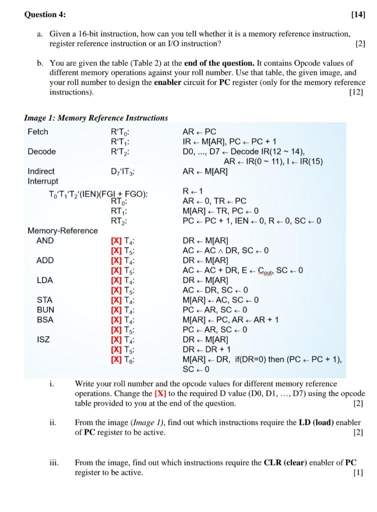
Question: My id is 201014111 and my opcode value 101 001 100 011 010 000 110 Question 4: [14] a. Given a 16-bit instruction, how can
![011 010 000 110 Question 4: [14] a. Given a 16-bit instruction,](https://dsd5zvtm8ll6.cloudfront.net/si.experts.images/questions/2024/09/66fa6aac8870a_34066fa6aac28ead.jpg)
My id is 201014111 and my opcode value 101 001 100 011 010 000 110
Question 4: [14] a. Given a 16-bit instruction, how can you tell whether it is a memory reference instruction, register reference instruction or an I/O instruction? [2] b. You are given the table (Table 2) at the end of the question. It contains Opcode values of different memory operations against your roll number. Use that table, the given image, and your roll number to design the enabler circuit for PC register (only for the memory reference instructions). [12] R'T2: Image 1: Memory Reference Instructions Fetch R'To: ARPC RT: IR MAR), PC PC + 1 Decode DO, ..., D7 - Decode IR(12-14), ARIR(0 - 11), IIR(15) Indirect D'IT: ARM[AR] Interrupt R-1 To'T,'T '(IEN)(FGI+ FGO): RTO: AR-0, TR-PC RT: M[AR] TR, PC +0 RT 2: PC - PC + 1, IENO, RO, SC 0 Memory-Reference AND [X] TA: DR - M[AR] [X] T5: AC AC ADR, SCO ADD [X] TA DR M[AR] [X] T5: AC AC + DR, E + Cout, SC - 0 LDA [X] TA DR M[AR] [X] T5: AC DR, SCO STA [X] T.: M[AR] - AC, SC-0 BUN [X] TA: PC-AR, SCO BSA [X] TA M[AR] PC, AR AR + 1 [X] T5: PC AR, SC 0 ISZ [X] TA: DR MAR] [X] T5 DR DR + 1 [X] To: M[AR] - DR, if(DR=0) then (PC - PC + 1), SC 0 i. Write your roll number and the opcode values for different memory reference operations. Change the [X] to the required D value (DO, DI, ..., D7) using the opcode table provided to you at the end of the question. [2] ii. From the image (Image 1), find out which instructions require the LD (load) enabler of PC register to be active. [2] iii. From the image, find out which instructions require the CLR (clear) enabler of PC register to be active. [1] iv. From the image, find out which instructions require the INR (increment) enabler of PC register to be active. [1] V. Hence, find the overall equation for LD, CLR and INR of the DR register. [4] vi. Draw the circuit diagram using your answer to part (v). [2]
Step by Step Solution
There are 3 Steps involved in it

Get step-by-step solutions from verified subject matter experts