

Question: n, build and test a combinational logic circuit with four inputs -A, B, C, and D, that meets the following design specifications and implementation constraints.
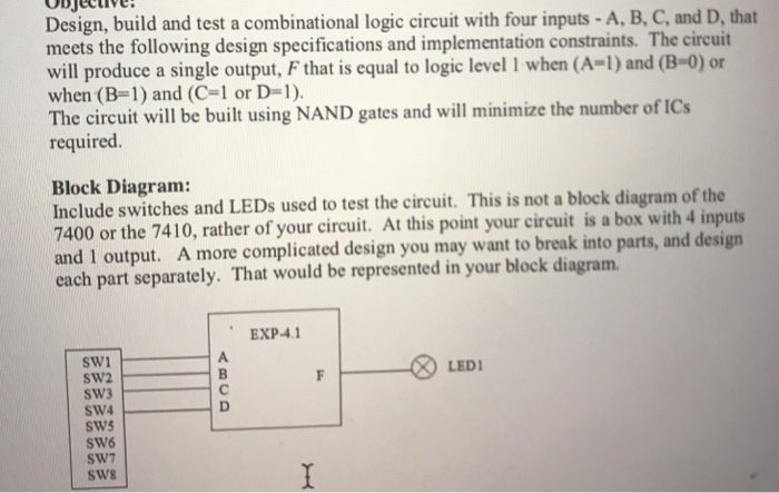

n, build and test a combinational logic circuit with four inputs -A, B, C, and D, that meets the following design specifications and implementation constraints. The circuit will produce a single output, F that is equal to logic level 1 when (A-1) and (B-0) or when (B-1) and (C-1 or D-1). The circuit will be built using NAND gates and will minimize the number of ICs required Block Diagram: Include switches and LEDs used to test the circuit. This is not a block diagram of the 7400 or the 7410, rather of your circuit. At this point your circuit is a box with 4 inputs and 1 output. A more complicated design you may want to break into parts, and each part separately. That would be represented in your block diagram. EXP-4.1 swi LEDI SW4 sw5 SW7 SWs Design Procedure: Should include the following components as you designed to meet the objective: 1. How you interpreted the objective as stated as a Boolean function. 2. Design rules to map the objective into a truth table and the truth table itself (O in your truth table matches your block diagram) 3. K-maps 4. Conversion of AND-OR to NAND-NAND using involution and DeMorgan's theorem Schematic Diagram: Inputs on Left, Outputs on Right (VO variables match your block diagram) Switch numbers indentified Pin numbers on Gate VO Parts List on the schematic
Step by Step Solution
There are 3 Steps involved in it

Get step-by-step solutions from verified subject matter experts