

Question: need help with the code for this problem. program in use: vivado mainly need the standard VHD code, but the test bench file will help
need help with the code for this problem. program in use: vivado
mainly need the standard VHD code, but the test bench file will help as well
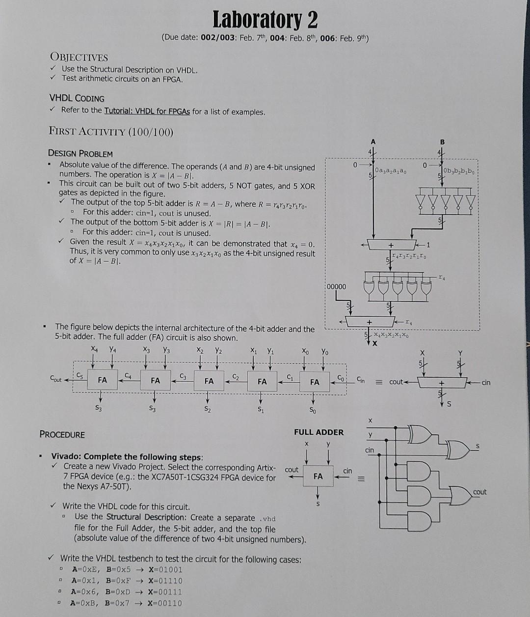
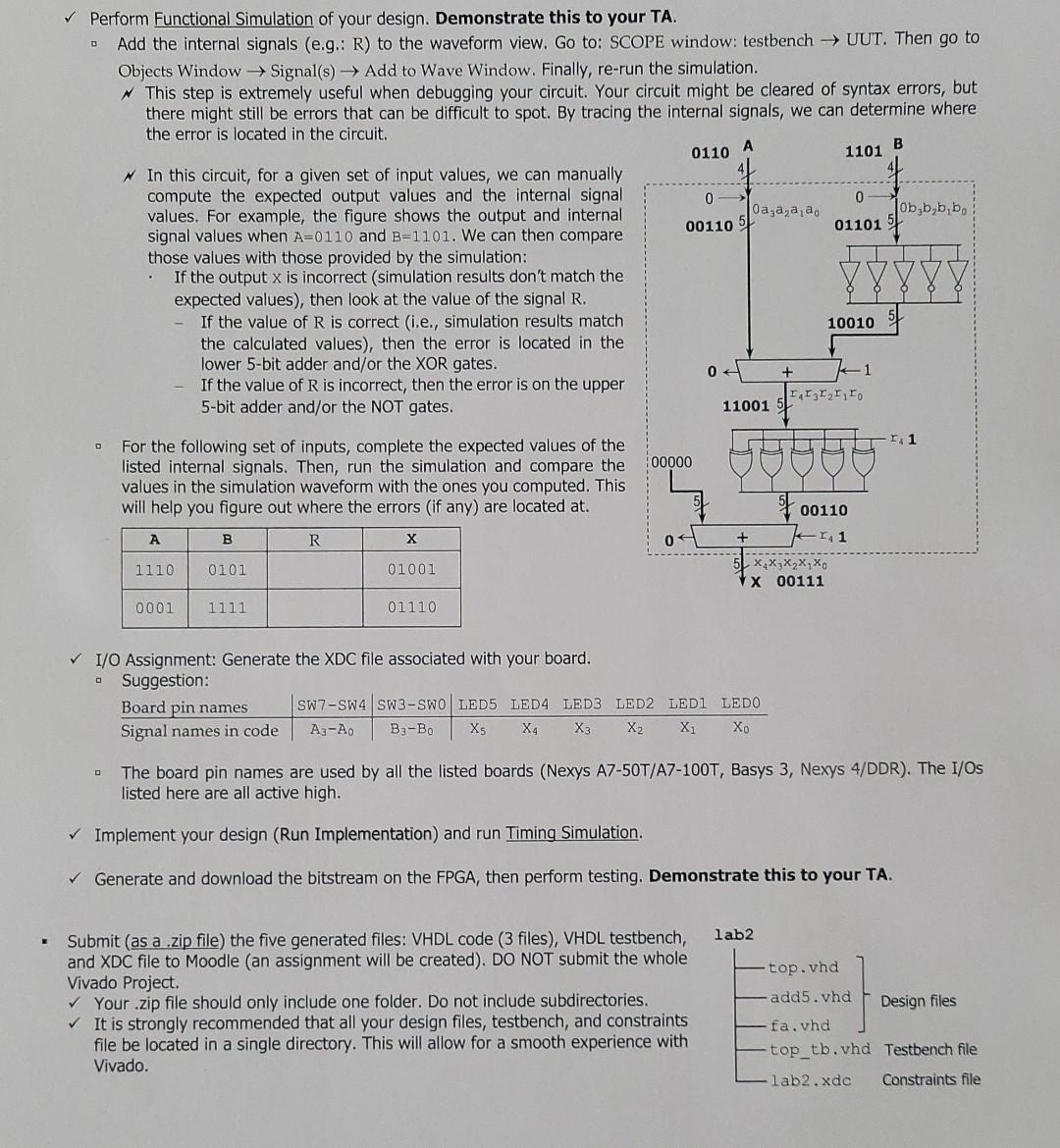
Laboratory 2 (Due date: 002/003: Feb. 7th, 004: Feb. 8th, 006: Feb. 9th) OBJECTIVES Use the Structural Description on VHDL. Test arithmetic circuits on an FPGA. VHDL CODING Refer to the Tutorial: VHDL for FPGAs for a list of examples. FIRST ACTIVITY (100/100) . 0 Oaza,a,a, Ob b b b DESIGN PROBLEM Absolute value of the difference. The operands (A and B) are 4-bit unsigned numbers. The operation is X = |A-BI. This circuit can be built out of two 5-bit adders, 5 NOT gates, and 5 XOR gates as depicted in the figure. The output of the top 5-bit adder is R=A-B, where R = 47372riro. For this adder: cin=1, cout is unused. The output of the bottom 5-bit adder is X = |R| = |A-BI. For this adder: cin=1, cout is unused. Given the result X = X4X3X2X1Xo, it can be demonstrated that x4 = 0. Thus, it is very common to only use X3X2X1X as the 4-bit unsigned result of X = |A-BI. 0 D I Iz Iz I, Io 14 00000 + The figure below depicts the internal architecture of the 4-bit adder and the 5-bit adder. The full adder (FA) circuit is also shown. X Y2 X2 Ya X Y2 X Xo xx, x, x, xo Yo Cout FA C4 C3 C2 Ci FA FA FA FA Cin cout cin S S3 S3 S2 S1 So X PROCEDURE FULL ADDER cin Vivado: Complete the following steps: Create a new Vivado Project. Select the corresponding Artix- 7 FPGA device (e.g.: the XC7A50T-1CSG324 FPGA device for the Nexys A7-50T). cout cin FA = cout Write the VHDL code for this circuit. Use the Structural Description: Create a separate .vhd file for the Full Adder, the 5-bit adder, and the top file (absolute value of the difference of two 4-bit unsigned numbers). Write the VHDL testbench to test the circuit for the following cases: A=0xE, B=0x5 X=01001 A=0xl, B=0xF X=01110 A=0x6, B=0xD X=00111 A=0xB, B=0x7 X=00110 O 1101 Perform Functional Simulation of your design. Demonstrate this to your TA. Add the internal signals (e.g.: R) to the waveform view. Go to: SCOPE window: testbench UUT. Then go to Objects Window Signal(s) Add to Wave Window. Finally, re-run the simulation. This step is extremely useful when debugging your circuit. Your circuit might be cleared of syntax errors, but there might still be errors that can be difficult to spot. By tracing the internal signals, we can determine where the error is located in the circuit. A B 0110 w In this circuit, for a given set of input values, we can manually compute the expected output values and the internal signal 0 0 values. For example, the figure shows the output and internal 0a,a,a,a, Ob bb,bo signal values when A=0110 and B=1101. We can then compare 00110 5 011015 those values with those provided by the simulation: If the output x is incorrect (simulation results don't match the expected values), then look at the value of the signal R. If the value of R is correct (i.e., simulation results match 10010 the calculated values), then the error is located in the lower 5-bit adder and/or the XOR gates. 0 If the value of R is incorrect, then the error is on the upper 5-bit adder and/or the NOT gates. II I I, Io 11001 + 1.1 00000 For the following set of inputs, complete the expected values of the listed internal signals. Then, run the simulation and compare the values in the simulation waveform with the ones you computed. This will help you figure out where the errors (if any) are located at. 00110 A B R 04 + -141 1110 0101 01001 5 X X X X X X 00111 0001 01110 I/O Assignment: Generate the XDC file associated with your board. Suggestion: Board pin names SW7-SW4 SW3-SWOLED5 LED4 LED3 LED2 LEDI LEDO Signal names in code A3-Ao B-Bo Xs X4 X3 X2 X Xo The board pin names are used by all the listed boards (Nexys A7-50T/A7-100T, Basys 3, Nexys 4/DDR). The I/Os listed here are all active high. Implement your design (Run Implementation) and run Timing Simulation. Generate and download the bitstream on the FPGA, then perform testing. Demonstrate this to your TA. lab2 top.vhd Submit (as a .zip file) the five generated files: VHDL code (3 files), VHDL testbench, and XDC file to Moodle (an assignment will be created). DO NOT submit the whole Vivado Project. Your .zip file should only include one folder. Do not include subdirectories. It is strongly recommended that all your design files, testbench, and constraints file be located in a single directory. This will allow for a smooth experience with Vivado. add5.vhd Design files fa.vhd top_tb.vhd Testbench file lab2.xde Constraints file Laboratory 2 (Due date: 002/003: Feb. 7th, 004: Feb. 8th, 006: Feb. 9th) OBJECTIVES Use the Structural Description on VHDL. Test arithmetic circuits on an FPGA. VHDL CODING Refer to the Tutorial: VHDL for FPGAs for a list of examples. FIRST ACTIVITY (100/100) . 0 Oaza,a,a, Ob b b b DESIGN PROBLEM Absolute value of the difference. The operands (A and B) are 4-bit unsigned numbers. The operation is X = |A-BI. This circuit can be built out of two 5-bit adders, 5 NOT gates, and 5 XOR gates as depicted in the figure. The output of the top 5-bit adder is R=A-B, where R = 47372riro. For this adder: cin=1, cout is unused. The output of the bottom 5-bit adder is X = |R| = |A-BI. For this adder: cin=1, cout is unused. Given the result X = X4X3X2X1Xo, it can be demonstrated that x4 = 0. Thus, it is very common to only use X3X2X1X as the 4-bit unsigned result of X = |A-BI. 0 D I Iz Iz I, Io 14 00000 + The figure below depicts the internal architecture of the 4-bit adder and the 5-bit adder. The full adder (FA) circuit is also shown. X Y2 X2 Ya X Y2 X Xo xx, x, x, xo Yo Cout FA C4 C3 C2 Ci FA FA FA FA Cin cout cin S S3 S3 S2 S1 So X PROCEDURE FULL ADDER cin Vivado: Complete the following steps: Create a new Vivado Project. Select the corresponding Artix- 7 FPGA device (e.g.: the XC7A50T-1CSG324 FPGA device for the Nexys A7-50T). cout cin FA = cout Write the VHDL code for this circuit. Use the Structural Description: Create a separate .vhd file for the Full Adder, the 5-bit adder, and the top file (absolute value of the difference of two 4-bit unsigned numbers). Write the VHDL testbench to test the circuit for the following cases: A=0xE, B=0x5 X=01001 A=0xl, B=0xF X=01110 A=0x6, B=0xD X=00111 A=0xB, B=0x7 X=00110 O 1101 Perform Functional Simulation of your design. Demonstrate this to your TA. Add the internal signals (e.g.: R) to the waveform view. Go to: SCOPE window: testbench UUT. Then go to Objects Window Signal(s) Add to Wave Window. Finally, re-run the simulation. This step is extremely useful when debugging your circuit. Your circuit might be cleared of syntax errors, but there might still be errors that can be difficult to spot. By tracing the internal signals, we can determine where the error is located in the circuit. A B 0110 w In this circuit, for a given set of input values, we can manually compute the expected output values and the internal signal 0 0 values. For example, the figure shows the output and internal 0a,a,a,a, Ob bb,bo signal values when A=0110 and B=1101. We can then compare 00110 5 011015 those values with those provided by the simulation: If the output x is incorrect (simulation results don't match the expected values), then look at the value of the signal R. If the value of R is correct (i.e., simulation results match 10010 the calculated values), then the error is located in the lower 5-bit adder and/or the XOR gates. 0 If the value of R is incorrect, then the error is on the upper 5-bit adder and/or the NOT gates. II I I, Io 11001 + 1.1 00000 For the following set of inputs, complete the expected values of the listed internal signals. Then, run the simulation and compare the values in the simulation waveform with the ones you computed. This will help you figure out where the errors (if any) are located at. 00110 A B R 04 + -141 1110 0101 01001 5 X X X X X X 00111 0001 01110 I/O Assignment: Generate the XDC file associated with your board. Suggestion: Board pin names SW7-SW4 SW3-SWOLED5 LED4 LED3 LED2 LEDI LEDO Signal names in code A3-Ao B-Bo Xs X4 X3 X2 X Xo The board pin names are used by all the listed boards (Nexys A7-50T/A7-100T, Basys 3, Nexys 4/DDR). The I/Os listed here are all active high. Implement your design (Run Implementation) and run Timing Simulation. Generate and download the bitstream on the FPGA, then perform testing. Demonstrate this to your TA. lab2 top.vhd Submit (as a .zip file) the five generated files: VHDL code (3 files), VHDL testbench, and XDC file to Moodle (an assignment will be created). DO NOT submit the whole Vivado Project. Your .zip file should only include one folder. Do not include subdirectories. It is strongly recommended that all your design files, testbench, and constraints file be located in a single directory. This will allow for a smooth experience with Vivado. add5.vhd Design files fa.vhd top_tb.vhd Testbench file lab2.xde Constraints file
Step by Step Solution
There are 3 Steps involved in it

Get step-by-step solutions from verified subject matter experts