

Question: I'm not asking for help with the code I have all the code thanks to previous labs but I want help with the diagrams. Deliverables

 I'm not asking for help with the code I have all the code thanks to previous labs but I want help with the diagrams.
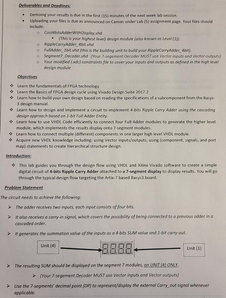
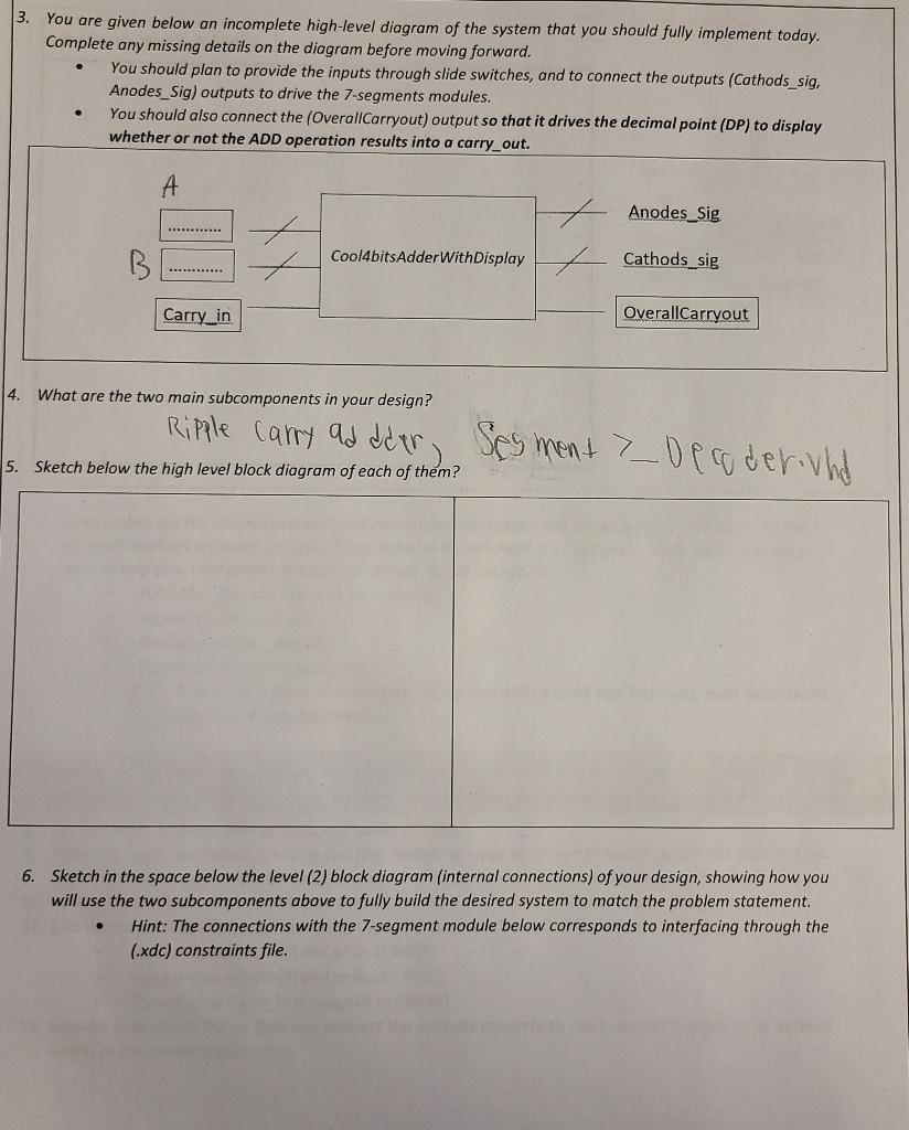
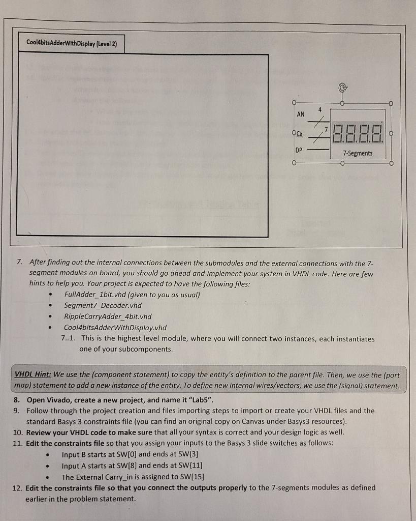
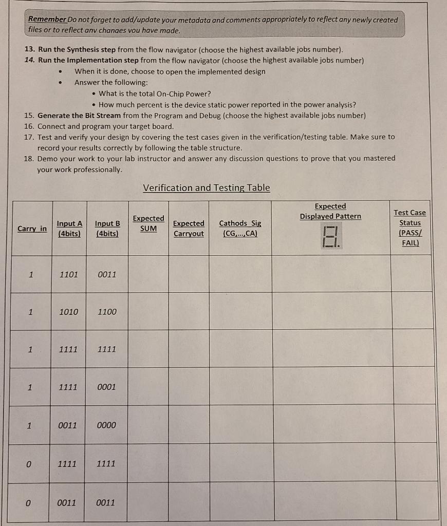
Deliverables and Deadlines: - Demoing your results is due in the first (15) minutes of the next week lab session. - Uploading your files is due as announced on Canvas under Lab (5) assignment page. Your files should include: Cool4bitsAdderWithDisplay.vhd - (This is your highest level) design module (also known as Level (1)). RippleCarryAdder_4bit.vhd FullAdder__1bit.vhd (this is the building unit to build your RippleCarryAdder_ 4 bit). Segment7_Decoder.vhd (Your 7-segement Decoder MUST use Vector inputs and Vector outputs) Your modified (.xdc) constraints file to cover your inputs and outputs as defined in the high level design module Objectives * Learn the fundamentals of FPGA technology * Learn the Basics of FPGA design cycle using Vivado Design Suite 2017.2 * Learn how to build your own design based on reading the specifications of a subcomponent from the Basys3 design manual. *- Learn how to design and implement a circuit to implement 4-bits Ripple Carry Adder using the cascading design approach based on 1-bit Full Adder Entity. * Learn how to use VHDL Code efficiently to connect four Full-Adder modules to generate the higher level module, which implements the results display onto 7-segment modules. *. Learn how to connect multiple (different) components in one larger high level VHDL module. * Acquire new VHDL knowledge including: using Vector inputs/outputs, using (component, signals, and port map) statements to create hierarchical structure design. Introduction: *. This lab guides you through the design flow using VHDL and Xilinx Vivado software to create a simple digital circuit of 4-bits Ripple Carry Adder attached to a 7-segment display to display results. You will go through the typical design flow targeting the Artix- 7 based Basys 3 board. Problem Statement The circuit needs to achieve the following: The adder receives two inputs, each input consists of four bits. It also receives a carry-in signal, which covers the possibility of being connected to a previous adder in a cascaded order. It generates the summation value of the inputs as a 4-bits SUM value and 1-bit carry-out. The resulting SUM should be displayed on the segment 7 modules, on UNIT (4) ONLY. (Your 7-segement Decoder MUST use Vector inputs and Vector outputs) Use the 7-segments' decimal point (DP) to represent/display the external Carry_out signal whenever applicable. For all inputs and outputs, the order of the bits matches the little endian method so that the least significant bit (LSB) is at the farthest right side and the most significant bit (MSB) is located at the farthest left side. Lab Instructions: 1. Sketch below the high level block diagram of the 4-bit Ripple Carry Adder showing the system inputs and outputs. 2. Sketch below the Level (2) (internal block diagram) of the 4-bit Ripple Carry Adder showing what the 4-bit Adder consists of internally. [You will use the Cascading design approach to implement the internals based on 1-bit Full Adder modules]. 3. You are given below an incomplete high-level diagram of the system that you should fully implement today. Complete any missing details on the diagram before moving forward. - You should plan to provide the inputs through slide switches, and to connect the outputs (Cathods_sig, Anodes_Sig) outputs to drive the 7 -segments modules. - You should also connect the (OverallCarryout) output so that it drives the decimal point (DP) to display whether or not the ADD operation results into a carry_out. 4. What are the two main subcomponents in your design? 6. Sketch in the space below the level (2) block diagram (internal connections) of your design, showing how you will use the two subcomponents above to fully build the desired system to match the problem statement. - Hint: The connections with the 7-segment module below corresponds to interfacing through the (.xdc) constraints file. 7. After finding out the internal connections between the submodules and the external connections with the 7 segment modules on board, you should go ahead and implement your system in VHDL code. Here are few hints to help you. Your project is expected to have the following files: - FullAdder_1bit.vhd (given to you as usual) - Segment7_Decoder.vhd - RippleCarryAdder_4bit.vhd - Cool4bitsAdderWithDisplay.vhd 7..1. This is the highest level module, where you will connect two instances, each instantiates one of your subcomponents. VHDL Hint: We use the (component statement) to copy the entity's definition to the parent file. Then, we use the (port map) statement to add a new instance of the entity. To define new internal wires/vectors, we use the (signal) statement. 8. Open Vivado, create a new project, and name it "Lab5". 9. Follow through the project creation and files importing steps to import or create your VHDL files and the standard Basys 3 constraints file (you can find an original copy on Canvas under Basys 3 resources). 10. Review your VHDL code to make sure that all your syntax is correct and your design logic as well. 11. Edit the constraints file so that you assign your inputs to the Basys 3 slide switches as follows: - Input B starts at SW[0] and ends at SW\{3] - Input A starts at SW[8] and ends at SW\{11] - The External Carry_in is assigned to SW[15] 12. Edit the constraints file so that you connect the outputs properly to the 7-segments modules as defined earlier in the problem statement. Remember Do not forget to add/update your metadata and comments appropriately to reflect any newly created files or to reflect anv chanaes vou have made. 13. Run the Synthesis step from the flow navigator (choose the highest available jobs number). 14. Run the Implementation step from the flow navigator (choose the highest available jobs number) - When it is done, choose to open the implemented design - Answer the following: - What is the total On-Chip Power? - How much percent is the device static power reported in the power analysis? 15. Generate the Bit Stream from the Program and Debug (choose the highest available jobs number) 16. Connect and program your target board. 17. Test and verify your design by covering the test cases given in the verification/testing table. Make sure to record your results correctly by following the table structure. 18. Demo your work to your lab instructor and answer any discussion questions to prove that you mastered your work professionally. Verification and Testing Table Deliverables and Deadlines: - Demoing your results is due in the first (15) minutes of the next week lab session. - Uploading your files is due as announced on Canvas under Lab (5) assignment page. Your files should include: Cool4bitsAdderWithDisplay.vhd - (This is your highest level) design module (also known as Level (1)). RippleCarryAdder_4bit.vhd FullAdder__1bit.vhd (this is the building unit to build your RippleCarryAdder_ 4 bit). Segment7_Decoder.vhd (Your 7-segement Decoder MUST use Vector inputs and Vector outputs) Your modified (.xdc) constraints file to cover your inputs and outputs as defined in the high level design module Objectives * Learn the fundamentals of FPGA technology * Learn the Basics of FPGA design cycle using Vivado Design Suite 2017.2 * Learn how to build your own design based on reading the specifications of a subcomponent from the Basys3 design manual. *- Learn how to design and implement a circuit to implement 4-bits Ripple Carry Adder using the cascading design approach based on 1-bit Full Adder Entity. * Learn how to use VHDL Code efficiently to connect four Full-Adder modules to generate the higher level module, which implements the results display onto 7-segment modules. *. Learn how to connect multiple (different) components in one larger high level VHDL module. * Acquire new VHDL knowledge including: using Vector inputs/outputs, using (component, signals, and port map) statements to create hierarchical structure design. Introduction: *. This lab guides you through the design flow using VHDL and Xilinx Vivado software to create a simple digital circuit of 4-bits Ripple Carry Adder attached to a 7-segment display to display results. You will go through the typical design flow targeting the Artix- 7 based Basys 3 board. Problem Statement The circuit needs to achieve the following: The adder receives two inputs, each input consists of four bits. It also receives a carry-in signal, which covers the possibility of being connected to a previous adder in a cascaded order. It generates the summation value of the inputs as a 4-bits SUM value and 1-bit carry-out. The resulting SUM should be displayed on the segment 7 modules, on UNIT (4) ONLY. (Your 7-segement Decoder MUST use Vector inputs and Vector outputs) Use the 7-segments' decimal point (DP) to represent/display the external Carry_out signal whenever applicable. For all inputs and outputs, the order of the bits matches the little endian method so that the least significant bit (LSB) is at the farthest right side and the most significant bit (MSB) is located at the farthest left side. Lab Instructions: 1. Sketch below the high level block diagram of the 4-bit Ripple Carry Adder showing the system inputs and outputs. 2. Sketch below the Level (2) (internal block diagram) of the 4-bit Ripple Carry Adder showing what the 4-bit Adder consists of internally. [You will use the Cascading design approach to implement the internals based on 1-bit Full Adder modules]. 3. You are given below an incomplete high-level diagram of the system that you should fully implement today. Complete any missing details on the diagram before moving forward. - You should plan to provide the inputs through slide switches, and to connect the outputs (Cathods_sig, Anodes_Sig) outputs to drive the 7 -segments modules. - You should also connect the (OverallCarryout) output so that it drives the decimal point (DP) to display whether or not the ADD operation results into a carry_out. 4. What are the two main subcomponents in your design? 6. Sketch in the space below the level (2) block diagram (internal connections) of your design, showing how you will use the two subcomponents above to fully build the desired system to match the problem statement. - Hint: The connections with the 7-segment module below corresponds to interfacing through the (.xdc) constraints file. 7. After finding out the internal connections between the submodules and the external connections with the 7 segment modules on board, you should go ahead and implement your system in VHDL code. Here are few hints to help you. Your project is expected to have the following files: - FullAdder_1bit.vhd (given to you as usual) - Segment7_Decoder.vhd - RippleCarryAdder_4bit.vhd - Cool4bitsAdderWithDisplay.vhd 7..1. This is the highest level module, where you will connect two instances, each instantiates one of your subcomponents. VHDL Hint: We use the (component statement) to copy the entity's definition to the parent file. Then, we use the (port map) statement to add a new instance of the entity. To define new internal wires/vectors, we use the (signal) statement. 8. Open Vivado, create a new project, and name it "Lab5". 9. Follow through the project creation and files importing steps to import or create your VHDL files and the standard Basys 3 constraints file (you can find an original copy on Canvas under Basys 3 resources). 10. Review your VHDL code to make sure that all your syntax is correct and your design logic as well. 11. Edit the constraints file so that you assign your inputs to the Basys 3 slide switches as follows: - Input B starts at SW[0] and ends at SW\{3] - Input A starts at SW[8] and ends at SW\{11] - The External Carry_in is assigned to SW[15] 12. Edit the constraints file so that you connect the outputs properly to the 7-segments modules as defined earlier in the problem statement. Remember Do not forget to add/update your metadata and comments appropriately to reflect any newly created files or to reflect anv chanaes vou have made. 13. Run the Synthesis step from the flow navigator (choose the highest available jobs number). 14. Run the Implementation step from the flow navigator (choose the highest available jobs number) - When it is done, choose to open the implemented design - Answer the following: - What is the total On-Chip Power? - How much percent is the device static power reported in the power analysis? 15. Generate the Bit Stream from the Program and Debug (choose the highest available jobs number) 16. Connect and program your target board. 17. Test and verify your design by covering the test cases given in the verification/testing table. Make sure to record your results correctly by following the table structure. 18. Demo your work to your lab instructor and answer any discussion questions to prove that you mastered your work professionally. Verification and Testing Table
Step by Step Solution
There are 3 Steps involved in it

Get step-by-step solutions from verified subject matter experts