

Question: Now, you are asked to implement 5 I/O devices (same as the devices in the previous question) that are addressed to the ports given (hex
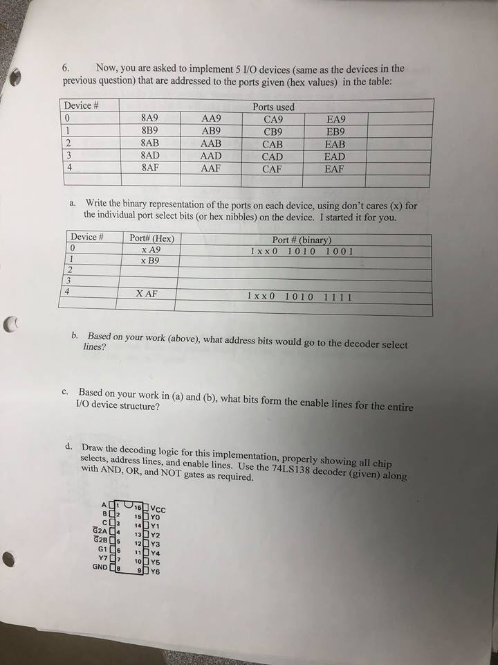
Now, you are asked to implement 5 I/O devices (same as the devices in the previous question) that are addressed to the ports given (hex values) in the table: Device # 8A9 8B9 8AB 8AD 8AF AA9 AB9 AAB AAD AAF Ports used CA9 CB9 CAB CAD CAF EA9 EB9 EAB EAD EAF 4 Write the binary representation of the ports on each device, using don't cares (x) for the individual port select bits (or hex nibbles) on the device. I started it for you. a. Device # x A9 x B9 1 x x 0 1010 1001 X AF 1 x x0 1010 1111 b. Based on your work (above), what address bits would go to the decoder select lines? Based on your work in (a) and (b), what bits form the enable lines for the entire I/O device structure? c. d. Draw the decoding logic for this implementation, properly showing all chip selects, address lines, and enable lines. Use the 74LS138 decoder (given) along with AND, OR, and NOT gates as required ?2 15DYO
Step by Step Solution
There are 3 Steps involved in it

Get step-by-step solutions from verified subject matter experts