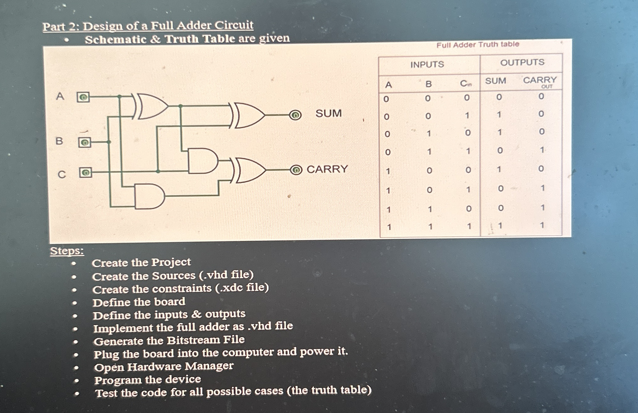
Question: Part 2 : Design of a Full Adder Circuit Schematic & Truth Table are given Full Adder Truth table table [ [ INPUTS ,
Part : Design of a Full Adder Circuit
Schematic & Truth Table are given
Full Adder Truth table
tableINPUTSOUTPUTSASUM,CARRY
Steps:
Create the Project
Create the Sources vhd file
Create the constraints xdc file
Define the board
Define the inputs & outputs
Implement the full adder as vhd file
Generate the Bitstream File
Plug the board into the computer and power it
Open Hardware Manager
Program the device
Test the code for all possible cases the truth table

Step by Step Solution
There are 3 Steps involved in it
1 Expert Approved Answer
Step: 1 Unlock


Question Has Been Solved by an Expert!
Get step-by-step solutions from verified subject matter experts
Step: 2 Unlock
Step: 3 Unlock


