

Question: Task 2 The ALU design will be simplified for this assignment. The block diagram of the ALU that you are required to design is given
Task
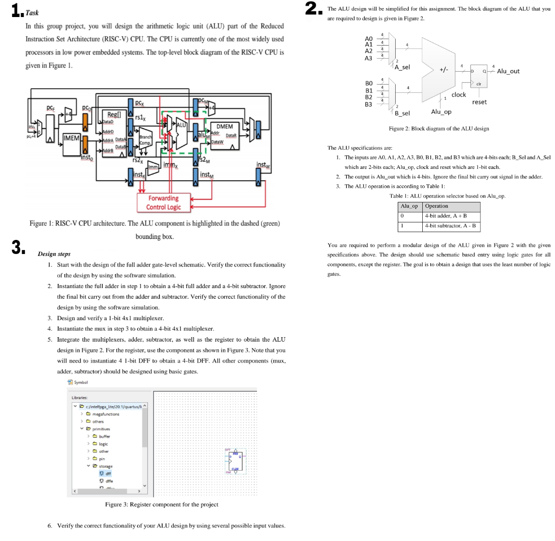
The ALU design will be simplified for this assignment. The block diagram of the ALU that you are required to design is given in Figure
In this group project, you will design the arithmetic logic unit ALU part of the Reduced Instruction Set Architecture RISCV CPU. The CPU is currently one of the most widely used processors in low power embedded systems. The toplevel block diagram of the RISCV CPU is given in Figure
Figure I: KISCV CPU architecture. The ALU component is highlighted in the dashed green bounding box.
Design steps
Start with the design of the full adder gatelevel schematic. Verify the correct functionality of the design by using the software simulation.
Instantiate the full adder in step to obtain a bit full adder and a bit subtractor. Ignore the final bit carry out from the adder and subtractor. Verify the correct functionality of the design by using the software simulation.
Design and verify a bit multiplexer.
Instantiate the mux in step to obtain a bit multiplexer.
Integrate the multiplexers, adder, subtractor, as well as the register to obtain the ALU design in Figure For the register, use the component as shown in Figure Note that you will need to instantiate bit DFF to obtain a bit DFF All other components mux adder, subtractor should be designed using basic gates.
Verify the correct functionality of your ALU design by using several possible input values.
The ALU specifications are:
The inputs are and which are bits each; Sel and which are bits each; Aluop clock and reset which are bit each.
The output is Aluout which is bits. Ignore the final bit carry out signal in the adder.
The ALU operation is according to Table I:
Table : ALU operation selector based on Aluop
tableAluopOperationbit adder, A Bbit subtractor, A B
You are required to perform a modular design of the ALU given in Figure with the given specifications above. The design should use schematic based entry using logic gates for all components, except the register. The goal is to obtain a design that uses the least number of logic gates.
please use pen and paper to solve it use deeds
Step by Step Solution
There are 3 Steps involved in it
1 Expert Approved Answer
Step: 1 Unlock

Question Has Been Solved by an Expert!
Get step-by-step solutions from verified subject matter experts
Step: 2 Unlock
Step: 3 Unlock