

Question: please answer 1,2 and 3 7. Experimental work: Design a carry ripple 4 bits as indicate the block diagram in the following figure. Use LEDs
please answer 1,2 and 3
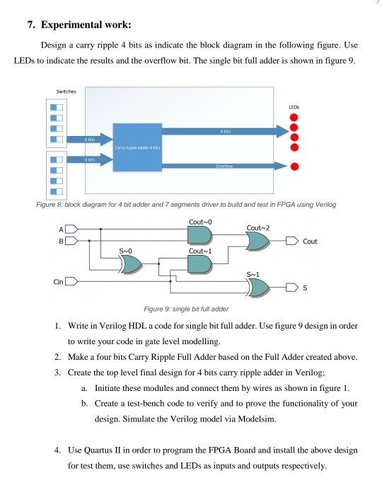
7. Experimental work: Design a carry ripple 4 bits as indicate the block diagram in the following figure. Use LEDs to indicate the results and the overflow bit. The single bit full adder is shown in figure 9. ople a re DES Figure 8: block diagram for 4 bit adder and 7 segments driver to build and test in FPGA using Verlog Couto Cout2 Cout Cout-1 Figure 9: single bit fulladder 1. Write in Verilog HDL a code for single bit full adder. Use figure 9 design in order to write your code in gate level modelling. 2. Make a four bits Carry Ripple Full Adder based on the Full Adder created above. 3. Create the top level final design for 4 bits carry ripple adder in Verilog; a. Initiate these modules and connect them by wires as shown in figure 1. b. Create a test-bench code to verify and to prove the functionality of your design. Simulate the Verilog model via Modelsim. 4. Use Quartus II in order to program the FPGA Board and install the above design for test them, use switches and LEDs as inputs and outputs respectively
Step by Step Solution
There are 3 Steps involved in it

Get step-by-step solutions from verified subject matter experts