

Question: Please create a RICS based program in logisim . Please follow the given instructions. Program Counter Design The Program Register ( PR ) is inside
Please create a RICS based program in logisim Please follow the given instructions. Program Counter Design
The Program Register PR is
inside the Program Counter PC
Its output will change it based on
feedback from the instruction
being executed
Set "trigger" to "falling edge" for
Program Register
PCMODE indicates whether to
INCREMENT, add the offset
IMMEDIATE, change it to
ABSOLUTE, or NO CHANGE
Example see inputs to MUX:
increment, immediate,
absoluteno change Instruction Storage
The program instructions will be
stored into a ROM x for
this simple CPU
Each address holds a single
instruction
Variables will be stored in a
separate RAM to simplify the design
The address will be provided by the
Program Register PR which is in
the Program Counter PC
component
The output will go to the instruction
decoder ID
Encode data using hexadecimal
one digit is bits Instruction Decode Part
RISC design attempts to simplify instruction
decode ID
Only wires!
Consistently place all instruction operands in the
same bits for all instruction types
Use "splitter" to break up busses into smaller
busseswires or combine smaller busseswires into
larger busses
Set "Bit Width In to and "Fan Out" is the number
of taps coming out of the splitter
Set which taps as assigned to which bits
Use "tunnels" to make connecting wires easier
Instruction Decode Part
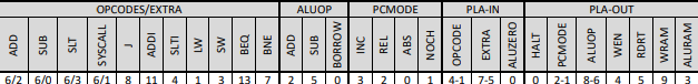
Need to use OPCODE, EXTRA, and ALUZERO to determine how to
execute instructions
Can use a LookUpTable LUT to determine proper outputs
Better than creating custom logic circuit remember the segment
decoder from DLD
Based on figure, LUT would be at least a bit input resulting in rows
Instead use Programmable Logic Array PLA
Better than LUT as it can have in input patterns
Your input patterns will have s in a number of places
Input signal to the PLA must not contain s or the output will be s
This CPU will only have PLA rows
The rows can be in any order the order is not important
PLAOUT will be split up to drive control signals of the remaining
circuit
Can not have s in outputs, must set to something see specifications
Reserve bits for EXTRA in PLA it is currently set higher bit to
for nowRegister File Design
Able to read registers per clock
Set RIN for register to read
output at ROUT"
Same for RIN and ROUT"
Able to write to one register per
clock
Apply data to "DATAIN"
Set "WINDEX" to register to write to
Goes through a decoder with enable;
all outputs set to on disabled
Set "WENABLE" to to write
No r; hard set to at output MUX
Set "trigger" to "falling edge" for
registers
ALU Design
Build your own ALU
Based heavily on Register File
Have a single MUX just before output
ALUOP should be bits for expansion
total modes possible
OIN is register value of RS and
OIN is register value of RT
Three modes necessary for now:
Add: ALUOUTOINOIN
Subtract: ALUOUTOINOIN
Borrow: ALUOUT if OINOIN otherwise
Take b out" from subtractor above, extend to bits with ZERO extension
ALUZERO output should be high if ALUOUT is zero use a comparator
For example: ALUOP is for ADD, for SUBTRACT, and for BORROW
Step by Step Solution
There are 3 Steps involved in it
1 Expert Approved Answer
Step: 1 Unlock

Question Has Been Solved by an Expert!
Get step-by-step solutions from verified subject matter experts
Step: 2 Unlock
Step: 3 Unlock