Question: PLEASE DO NOT USE AI TOOLS LIKE CHATGPT TO ANSWER. Since your circuit handles only BCD digits, check for the cases when the input x
PLEASE DO NOT USE AI TOOLS LIKE CHATGPT TO ANSWER. Since your circuit handles only BCD digits, check for the cases when the input or is greater than nine.
If this occurs, indicate an error by turning on the red light
Use ModelSim to simulate and debug your Verilog code. Make sure that you produce the correct output
values for all possible results of the BCD addition.
A top.v file is provided in the design files for this exercise, for use with the DESim tool. To use the top.v file
directly, declare your Verilog module as:
module partSW LEDR, HEX HEX HEX HEX HEX HEX;
input : SW;
output : LEDR;
output : HEX HEX HEX HEX HEX HEX;
endmodule
After you have finished testing your Verilog code using simulation, create a new Quartus project for your
adder.
Include the necessary pin assignments for the DESoC board, compile the circuit, and download it into the
FPGA chip.
Test your circuit by trying different values for numbers and modue top CLOCK SW KEY, HEX HEX HEX HEX HEX HEX LEDR;
input CLOCK; DEseries MHz clock signa
input wire : SW; DEseries switches
input wire : KEY; DEseries pushbuttons
output wire : HEXO; DEseries HEX displays
output wire : HEX;
output wire : HEX;
output wire : HEX;
output wire : HEX;
output wire : HEX;
output wire : LEDR; DEseries LEDs
part USW: LEDR, HEX HEX HEX HEX HEX HEX;
endmodue
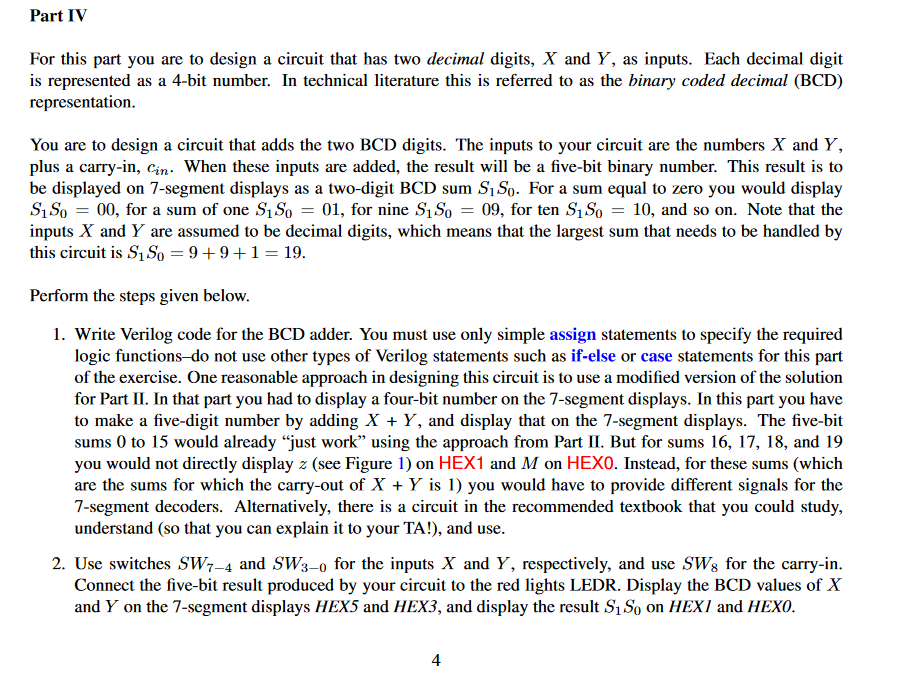
Part IV
For this part you are to design a circuit that has two decimal digits, and as inputs. Each decimal digit
is represented as a bit number. In technical literature this is referred to as the binary coded decimal BCD
representation.
You are to design a circuit that adds the two BCD digits. The inputs to your circuit are the numbers and
plus a carryin When these inputs are added, the result will be a fivebit binary number. This result is to
be displayed on segment displays as a twodigit BCD sum For a sum equal to zero you would display
for a sum of one for nine for ten and so on Note that the
inputs and are assumed to be decimal digits, which means that the largest sum that needs to be handled by
this circuit is
Perform the steps given below.
Write Verilog code for the BCD adder. You must use only simple assign statements to specify the required
logic functionsdo not use other types of Verilog statements such as ifelse or case statements for this part
of the exercise. One reasonable approach in designing this circuit is to use a modified version of the solution
for Part II In that part you had to display a fourbit number on the segment displays. In this part you have
to make a fivedigit number by adding and display that on the segment displays. The fivebit
sums to would already "just work" using the approach from Part II But for sums and
you would not directly display see Figure on HEX and on HEX Instead, for these sums which
are the sums for which the carryout of is you would have to provide different signals for the
segment decoders. Alternatively, there is a circuit in the recommended textbook that you could study,
understand so that you can explain it to your TA and use.
Use switches and for the inputs and respectively, and use for the carryin
Connect the fivebit result produced by your circuit to the red lights LEDR. Display the BCD values of
and on the segment displays HEX and HEX and display the result on HEXI and HEXO.

Step by Step Solution
There are 3 Steps involved in it
1 Expert Approved Answer
Step: 1 Unlock


Question Has Been Solved by an Expert!
Get step-by-step solutions from verified subject matter experts
Step: 2 Unlock
Step: 3 Unlock


