

Question: Please show step by step solution and explain. Thanks 3. SRAMs The following chip is a 8x8 bit RAM. Its logic symbol and function table
Please show step by step solution and explain. Thanks
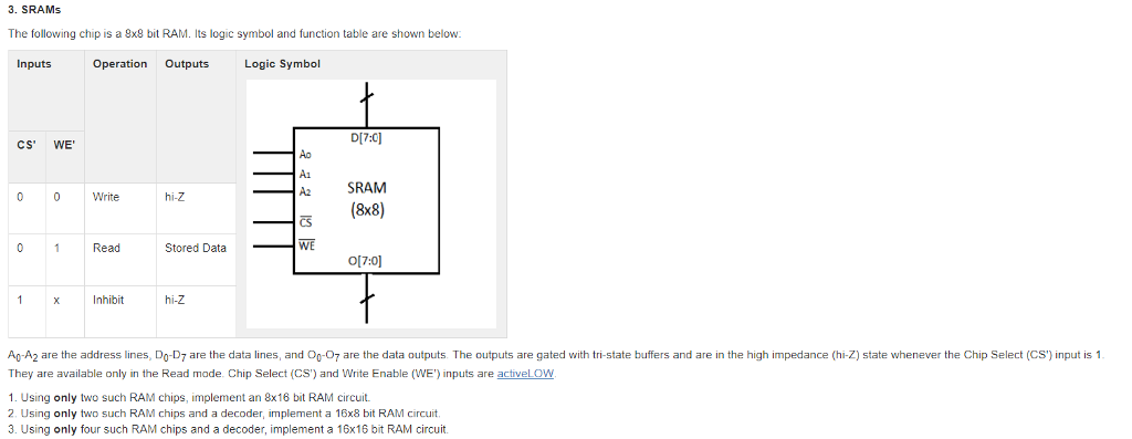
3. SRAMs The following chip is a 8x8 bit RAM. Its logic symbol and function table are shown below InputsOperation Outputs Logic Symbo DI7:0] CS WE Ao AT SRAM 00WritehiZ (8x8) 0 Read Stored Data WE 1 X nhbithi-Z AoA2 are the address lines, Do-D7 are the data lines, and O-0 are the data outputs. The outputs are gated with tri-state buffers and are in the high impedance (hi-Z) state whenever the Chip Select (CS') input is 1 They are available only in the Read mode. Chip Select (CS) and Write Enable (WE') inputs are activelOwW 1. Using only two such RAM chips, implement an 8x16 bit RAM circuit. 2. Using only two such RAM chips and a decoder, implement a 16x8 bit RAM circuit. 3. Using only four such RAM chips and a decoder, implement a 16x16 bit RAM circuit 3. SRAMs The following chip is a 8x8 bit RAM. Its logic symbol and function table are shown below InputsOperation Outputs Logic Symbo DI7:0] CS WE Ao AT SRAM 00WritehiZ (8x8) 0 Read Stored Data WE 1 X nhbithi-Z AoA2 are the address lines, Do-D7 are the data lines, and O-0 are the data outputs. The outputs are gated with tri-state buffers and are in the high impedance (hi-Z) state whenever the Chip Select (CS') input is 1 They are available only in the Read mode. Chip Select (CS) and Write Enable (WE') inputs are activelOwW 1. Using only two such RAM chips, implement an 8x16 bit RAM circuit. 2. Using only two such RAM chips and a decoder, implement a 16x8 bit RAM circuit. 3. Using only four such RAM chips and a decoder, implement a 16x16 bit RAM circuit
Step by Step Solution
There are 3 Steps involved in it

Get step-by-step solutions from verified subject matter experts