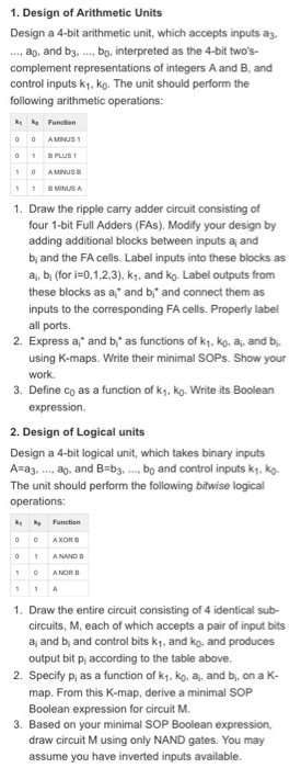
Question: Please show step by step solutions and explain if possible. Thank you so much 1. Design of Arithmetic Units Design a 4-bit arithmetic unit, which

1. Design of Arithmetic Units Design a 4-bit arithmetic unit, which accepts inputs a3. ..., ap, and b3. ..., bo, interpreted as the 4-bit two's- complement representations of integers A and B, and control inputs k1, ko. The unit should perform the following arithmetic operations: Funtin 10 AMINUSB B MINUS A 1. Draw the ripple carry adder circuit consisting of four 1-bit Full Adders (FAs). Modify your design by adding additional blocks between inputs a, and b and the FA cells. Label inputs into these blocks as ai, bi (for i=0, 1,2,3), k1, and k0. Label outputs from these blocks as a" and b and connect them as inputs to the corresponding FA cells. Properly label all ports. 2. Express af and b as functions of k1, ko, a, and b using K-maps. Write their minimal SOPs. Show your work 3. Define co as a function of k1, ko.Write its Boolean expression 2. Design of Logical units Design a 4-bit logical unit, which takes binary inputs Asa3-..., ao, and B-b3, , bo and control inputs kl The unit should perform the following bitwise logical operations: k, Function 0 0AXDR 10 A NOR B 11A 1. Draw the entire circuit consisting of 4 identical sub- circuits, M, each of which accepts a pair of input bits a, and b, and control bits k1, and ko, and produces output bit p according to the table above 2. Specify pi as a function of k1, ko, a, and bi, on a K- map. From this K-map, derive a minimal SOP Boolean expression for circuit M Based on your minimal SOP Boolean expression, draw circuit M using only NAND gates. You may assume you have inverted inputs available. 3
Step by Step Solution
There are 3 Steps involved in it

Get step-by-step solutions from verified subject matter experts


