

Question: please solve the question Q5.5 . JCL Inc.) JCL Inc. is a major chip manufacturing firm that sells its products to com- puter manufacturers like
please solve the question
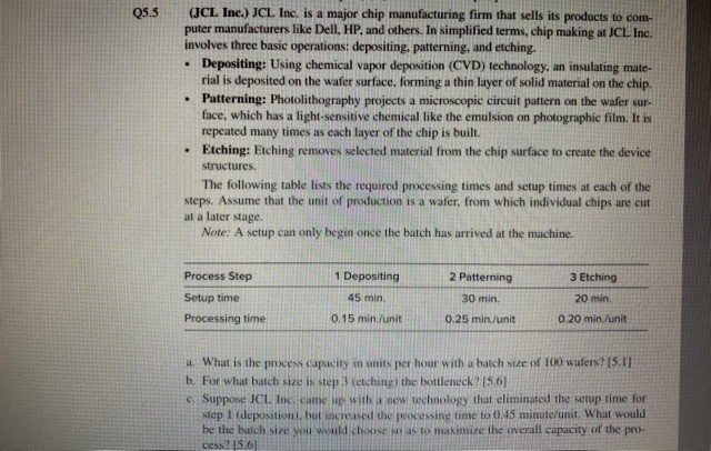
Q5.5 . JCL Inc.) JCL Inc. is a major chip manufacturing firm that sells its products to com- puter manufacturers like Dell, HP, and others. In simplified terms, chip making at JCL Inc. involves three basic operations: depositing. patterning, and etching. Depositing: Using chemical vapor deposition (CVD) technology, an insulating mate- rial is deposited on the wafer surface, forming a thin layer of solid material on the chip. Patterning: Photolithography projects a microscopic circuit pattern on the wafer sur face, which has a light-sensitive chemical like the emulsion on photographic film. It is repeated many times as each layer of the chip is built. Etching: Etching removes selected material from the chip surface to create the device structures, The following table lists the required processing times and setup times at each of the steps. Assume that the unit of production is a wafer, from which individual chips are cut at a later stage. Note: A setup can only begin once the batch has arrived at the machine. Process Step 1 Depositing 3 Etching 2 Patterning 30 min Setup time 20 min 45 min 0.15 min./unit Processing time 0.25 min./unit 0.20 min./unit a. What is the process capacity in units per hour with a batch size of 100 wafers[5.11 b. For what batch size is step 3 (etching the bottleneck? 15.61 & Suppose ICL Inc, cume up with a new technology that eliminated the setup time for step 1 (deposition, but creased the processing time to 0.45 minute/unit. What would be the batch size you would chose so as to maximize the overall capacity of the pro- cess? 15.6Step by Step Solution
There are 3 Steps involved in it
1 Expert Approved Answer
Step: 1 Unlock

Question Has Been Solved by an Expert!
Get step-by-step solutions from verified subject matter experts
Step: 2 Unlock
Step: 3 Unlock