

Question: plz solve this problem sir... VDD Rp RG Vps Vas FIGURE 4.32 Biasing the MOSFET using a large drain-to-gate feedback resis- tance, Ro. The circuit
plz solve this problem sir...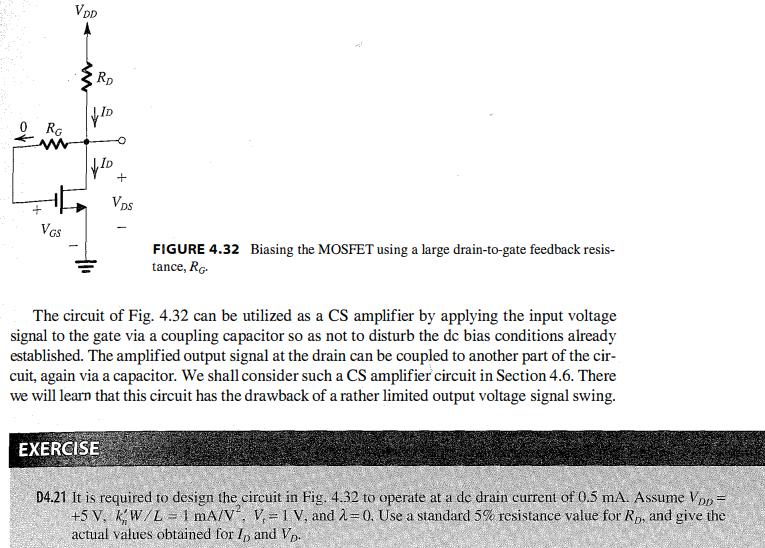
VDD Rp RG Vps Vas FIGURE 4.32 Biasing the MOSFET using a large drain-to-gate feedback resis- tance, Ro. The circuit of Fig. 4.32 can be utilized as a CS amplifier by applying the input voltage signal to the gate via a coupling capacitor so as not to disturb the de bias conditions already established. The amplified output signal at the drain can be coupled to another part of the cir- cuit, again via a capacitor. We shall consider such a CS amplifier circuit in Section 4.6. There we will learn that this circuit has the drawback of a rather limited output voltage signal swing. EXERCISE D4.21 It is required to design the circuit in Fig. 4.32 to operate at a de drain current of 0.5 mA. Assume Vpp = +5 V. KW/L =1 mA/V, V, = 1 V, and A=0. Use a standard 5% resistance value for Rp, and give the actual values obtained for I, and Vp.
Step by Step Solution
3.38 Rating (157 Votes )
There are 3 Steps involved in it
To design the circuit as described in Exercise D421 well follow these steps Given VDD 5 textV ID 05 ... View full answer

Get step-by-step solutions from verified subject matter experts