

Question: Plz write a C programming that follows the below pictures A MOSFET (Metal-Oxide-Semiconductor Field-Effect Transistor is an active electronic component that can be used either
Plz write a C programming that follows the below pictures 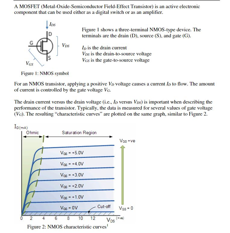
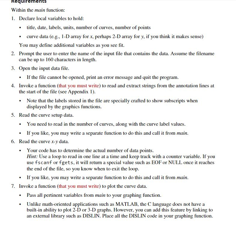
A MOSFET (Metal-Oxide-Semiconductor Field-Effect Transistor is an active electronic component that can be used either as a digital switch or as an amplifier IDs Figure 1 shows a three-terminal NMOS-type device. The terminals are the drain (D), source (S), and gate (G). VDs ID is the drain current VDs is the drain-to-source voltage VGs is the gate-to-source voltage GS Figure 1: NMos Symbol For an NMOS transistor, applying a positive VD voltage causes a current ID to flow. The amount of current is controlled by the gate voltage VG. The drain current versus the drain voltage (i.e., ID versus VDs) is important when describing the performance of the transistor. Typically, the data is measured for several values of gate voltage (VG). The resulting "characteristic curves" are plotted on the same graph, similar to Figure 2. D(mA) Saturation Region Ohmic GS +ve VGs 5.0V VGs 4.0V VGs 3.0V VGs 2.0V VGs 1.0V Cut-off 0V GS 10 12 We Figure 2: NMos characteristic curves A MOSFET (Metal-Oxide-Semiconductor Field-Effect Transistor is an active electronic component that can be used either as a digital switch or as an amplifier IDs Figure 1 shows a three-terminal NMOS-type device. The terminals are the drain (D), source (S), and gate (G). VDs ID is the drain current VDs is the drain-to-source voltage VGs is the gate-to-source voltage GS Figure 1: NMos Symbol For an NMOS transistor, applying a positive VD voltage causes a current ID to flow. The amount of current is controlled by the gate voltage VG. The drain current versus the drain voltage (i.e., ID versus VDs) is important when describing the performance of the transistor. Typically, the data is measured for several values of gate voltage (VG). The resulting "characteristic curves" are plotted on the same graph, similar to Figure 2. D(mA) Saturation Region Ohmic GS +ve VGs 5.0V VGs 4.0V VGs 3.0V VGs 2.0V VGs 1.0V Cut-off 0V GS 10 12 We Figure 2: NMos characteristic curves
Step by Step Solution
There are 3 Steps involved in it

Get step-by-step solutions from verified subject matter experts