

Question: Problem 2 : Adder Design ( 2 8 pts ) Consider a 2 4 - bit adder design based on the Carry - Bypass architecture.
Problem : Adder Design pts
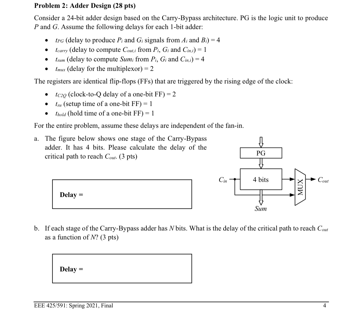
Consider a bit adder design based on the CarryBypass architecture. PG is the logic unit to produce and Assume the following delays for each bit adder:
delay to produce and signals from and
delay to compute from and :
Step by Step Solution
There are 3 Steps involved in it
1 Expert Approved Answer
Step: 1 Unlock

Question Has Been Solved by an Expert!
Get step-by-step solutions from verified subject matter experts
Step: 2 Unlock
Step: 3 Unlock