

Question: Problem 3 (25 pts) Field programmable gate arrays (FPGAs) such as the Altera Cyclone IV chip on the lab board use a structure known as
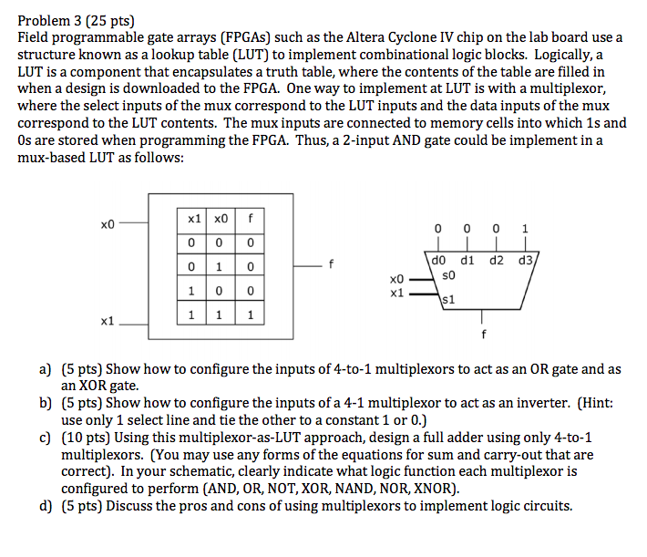
Problem 3 (25 pts) Field programmable gate arrays (FPGAs) such as the Altera Cyclone IV chip on the lab board use a structure known as a lookup table (LUT) to implement combinational logic blocks. Logically, a LUT is a component that encapsulates a truth table, where the contents of the table are filled in when a design is downloaded to the FPGA. One way to implement at LUT is with a multiplexor, where the select inputs of the mux correspond to the LUT inputs and the data inputs of the mux correspond to the LUT contents. The mux inputs are connected to memory cells into which 1s and 0s are stored when programming the FPGA. Thus, a 2-input AND gate could be implement in a mux-based LUT as follows: do d1 d2 d3 x0 1 00 a) (5 pts) Show how to configure the inputs of 4-to-1 multiplexors to act as an OR gate and as b) (5 pts) Show how to configure the inputs of a 4-1 multiplexor to act as an inverter. (Hint: c) (10 pts) Using this multiplexor-as-LUT approach, design a full adder using only 4-to-1 an XOR gate. use only 1 select line and tie the other to a constant1 or 0.) multiplexors. (You may use any forms of the equations for sum and carry-out that are correct). In your schematic, clearly indicate what logic function each multiplexor is configured to perform (AND, OR, NOT, XOR, NAND, NOR, XNOR) d) (5 pts) Discuss the pros and cons of using multiplexors to implement logic circuits. Problem 3 (25 pts) Field programmable gate arrays (FPGAs) such as the Altera Cyclone IV chip on the lab board use a structure known as a lookup table (LUT) to implement combinational logic blocks. Logically, a LUT is a component that encapsulates a truth table, where the contents of the table are filled in when a design is downloaded to the FPGA. One way to implement at LUT is with a multiplexor, where the select inputs of the mux correspond to the LUT inputs and the data inputs of the mux correspond to the LUT contents. The mux inputs are connected to memory cells into which 1s and 0s are stored when programming the FPGA. Thus, a 2-input AND gate could be implement in a mux-based LUT as follows: do d1 d2 d3 x0 1 00 a) (5 pts) Show how to configure the inputs of 4-to-1 multiplexors to act as an OR gate and as b) (5 pts) Show how to configure the inputs of a 4-1 multiplexor to act as an inverter. (Hint: c) (10 pts) Using this multiplexor-as-LUT approach, design a full adder using only 4-to-1 an XOR gate. use only 1 select line and tie the other to a constant1 or 0.) multiplexors. (You may use any forms of the equations for sum and carry-out that are correct). In your schematic, clearly indicate what logic function each multiplexor is configured to perform (AND, OR, NOT, XOR, NAND, NOR, XNOR) d) (5 pts) Discuss the pros and cons of using multiplexors to implement logic circuits
Step by Step Solution
There are 3 Steps involved in it

Get step-by-step solutions from verified subject matter experts