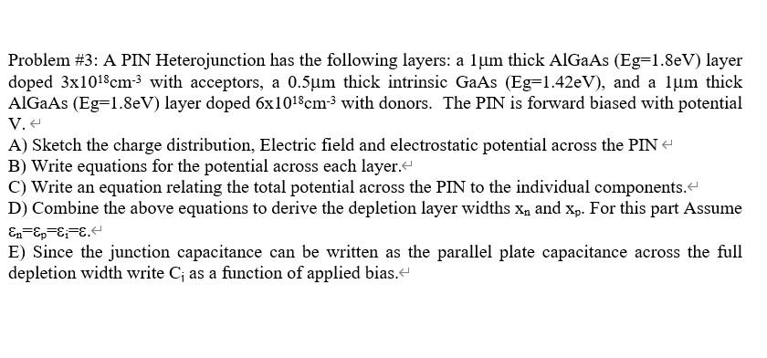
Question: Problem #3: A PIN Heterojunction has the following layers: a lum thick AlGaAs (Eg=1.8eV) layer doped 3x1018cm3 with acceptors, a 0.5um thick intrinsic GaAs (Eg=1.42eV),

Problem #3: A PIN Heterojunction has the following layers: a lum thick AlGaAs (Eg=1.8eV) layer doped 3x1018cm3 with acceptors, a 0.5um thick intrinsic GaAs (Eg=1.42eV), and a lum thick AlGaAs (Eg=1.8eV) layer doped 6x1018cm-3 with donors. The PIN is forward biased with potential V. A) Sketch the charge distribution, Electric field and electrostatic potential across the PIN B) Write equations for the potential across each layer.' C) Write an equation relating the total potential across the PIN to the individual components. D) Combine the above equations to derive the depletion layer widths Xn and Xp. For this part Assume &n=&p=&=E. E) Since the junction capacitance can be written as the parallel plate capacitance across the full depletion width write C as a function of applied bias. Problem #3: A PIN Heterojunction has the following layers: a lum thick AlGaAs (Eg=1.8eV) layer doped 3x1018cm3 with acceptors, a 0.5um thick intrinsic GaAs (Eg=1.42eV), and a lum thick AlGaAs (Eg=1.8eV) layer doped 6x1018cm-3 with donors. The PIN is forward biased with potential V. A) Sketch the charge distribution, Electric field and electrostatic potential across the PIN B) Write equations for the potential across each layer.' C) Write an equation relating the total potential across the PIN to the individual components. D) Combine the above equations to derive the depletion layer widths Xn and Xp. For this part Assume &n=&p=&=E. E) Since the junction capacitance can be written as the parallel plate capacitance across the full depletion width write C as a function of applied bias
Step by Step Solution
There are 3 Steps involved in it

Get step-by-step solutions from verified subject matter experts


