

Question: Problem 4 (10pts). A standard 32-register register file usually takes in a single 32-bit data input for writing to the register file, a selector bit
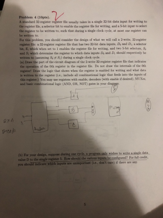
Problem 4 (10pts). A standard 32-register register file usually takes in a single 32-bit data input for writing to the register file, a selector bit to enable the register file for writing, and a 5-bit input to select the register to be written to, such that during a single clock cycle, at most one register can be written to. For this problem, you should consider the design of what we will call a 2-write, 32-register register file: a 32-register register file that has two 32-bit data inputs, Do and Di, a selector bit, E, which when set to 1 enables the register file for writing, and two 5-bit selectors, S and Si which determine the register to which data inputs Do and Di should respectively be written to (assuming So S1) during a single clock cycle. (a) Draw the part of the circuit diagram of the 2-write 32-register register file that indicates the operation of the 0th register in the register file. Do not draw the internals of the Oth register! Draw the logic that shows when the register is enabled for writing and what data is written to the register (i.e., include all combinational logic that feeds into the inputs of this register.) You may use registers with enable, decoders (with enable if desired), MUXes, and basic combinational logic (AND, OR, NOT) gates in your di (b) For your design, suppose during one cycle, a program only wishes to write a single data value D to the single register 5. How should the various inputs be configured? For full credit, you shoud indicate which inputs are unimportant (Le, don't care) if there are any. Problem 4 (10pts). A standard 32-register register file usually takes in a single 32-bit data input for writing to the register file, a selector bit to enable the register file for writing, and a 5-bit input to select the register to be written to, such that during a single clock cycle, at most one register can be written to. For this problem, you should consider the design of what we will call a 2-write, 32-register register file: a 32-register register file that has two 32-bit data inputs, Do and Di, a selector bit, E, which when set to 1 enables the register file for writing, and two 5-bit selectors, S and Si which determine the register to which data inputs Do and Di should respectively be written to (assuming So S1) during a single clock cycle. (a) Draw the part of the circuit diagram of the 2-write 32-register register file that indicates the operation of the 0th register in the register file. Do not draw the internals of the Oth register! Draw the logic that shows when the register is enabled for writing and what data is written to the register (i.e., include all combinational logic that feeds into the inputs of this register.) You may use registers with enable, decoders (with enable if desired), MUXes, and basic combinational logic (AND, OR, NOT) gates in your di (b) For your design, suppose during one cycle, a program only wishes to write a single data value D to the single register 5. How should the various inputs be configured? For full credit, you shoud indicate which inputs are unimportant (Le, don't care) if there are any
Step by Step Solution
There are 3 Steps involved in it

Get step-by-step solutions from verified subject matter experts