

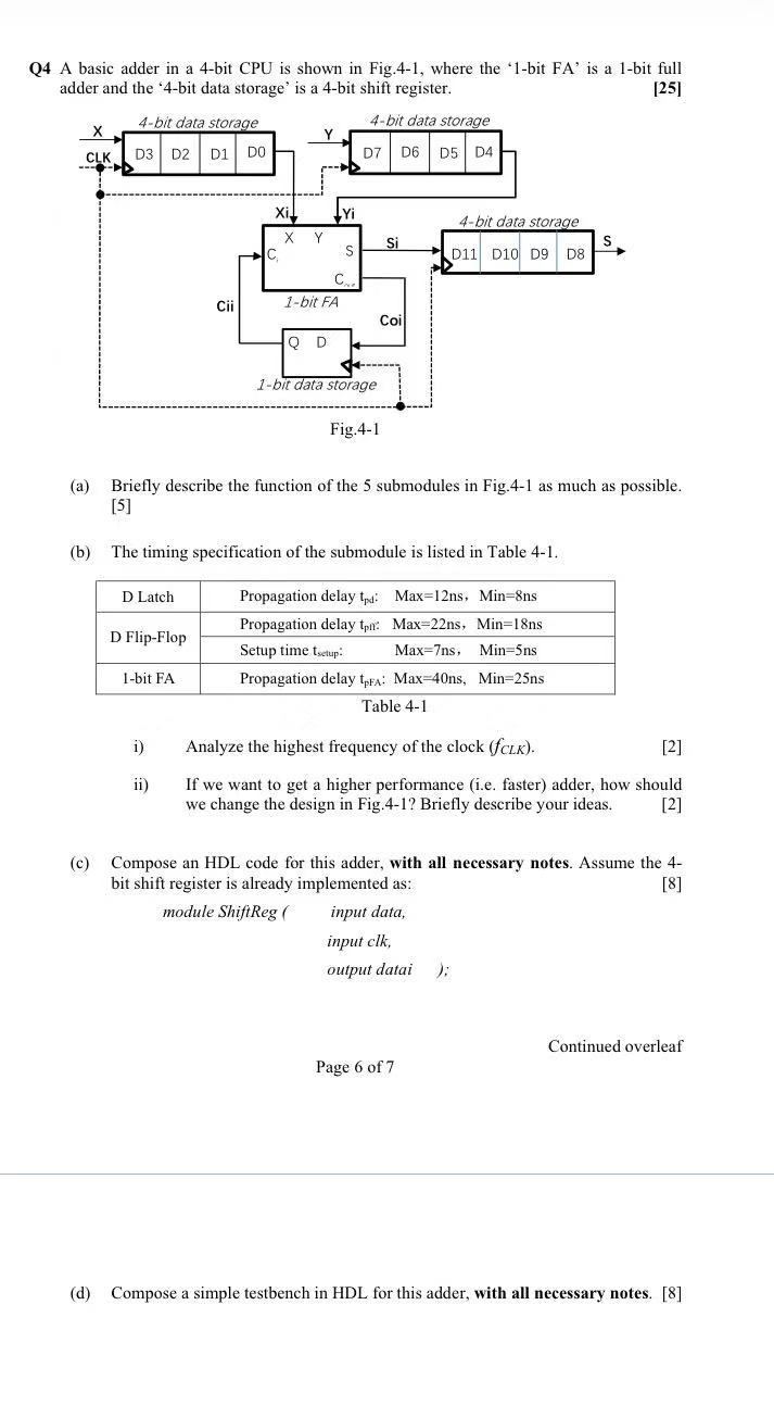
Question: Q 4 A basic adder in a 4 - bit CPU is shown in Fig . 4 - 1 , where the ' 1 -
Q A basic adder in a bit CPU is shown in Fig where the bit FA is a bit full adder and the bit data storage' is a bit shift register.
a Briefly describe the function of the submodules in Fig as much as possible.
b The timing specification of the submodule is listed in Table
tableD Latch,Propagation delay :Maxns MinnsD FlipFlop,Propagation delay tpri:,Maxns MinnsSetup time :Maxns Minnsbit FAPropagation delay :Maxns Minns
Table
i Analyze the highest frequency of the clock
ii If we want to get a higher performance ie faster adder, how should we change the design in Fig Briefly describe your ideas.
c Compose an HDL code for this adder, with all necessary notes. Assume the bit shift register is already implemented as:
module ShiftReg input data,
input clk
output datai ;
Page of
Continued overleaf
d Compose a simple testbench in HDL for this adder, with all necessary notes.
Step by Step Solution
There are 3 Steps involved in it
1 Expert Approved Answer
Step: 1 Unlock

Question Has Been Solved by an Expert!
Get step-by-step solutions from verified subject matter experts
Step: 2 Unlock
Step: 3 Unlock