

Question: QUESTION 1 Let's suppose that your embedded system has ROM, RAM, Device A, and Device B chips. The addresses are as shown in the following
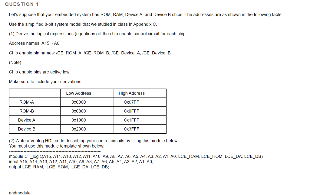
QUESTION 1 Let's suppose that your embedded system has ROM, RAM, Device A, and Device B chips. The addresses are as shown in the following table. Use the simplified 8-bit system model that we studied in class in Appendix C. (1) Derive the logical expressions (equations) of the chip enable control circuit for each chip. Address names: A15 - AO Chip enable pin names: /CE_ROM_A, ICE_ROM_B,/CE_Device_A, ICE_Device_B (Note) Chip enable pins are active low. Make sure to include your derivations Low Address High Address ROM-A Ox0000 Ox07FF ROM-B Ox0800 OXOFFF Device A Ox1000 Ox1FFF Device B Ox2000 Ox3FFF (2) Write a Verilog HDL code describing your control circuits by filling this module below. You must use this module template shown below: module CT_logic(A15, A14, A13, A12, A11, A10, A9, A8, A7, A6, A5, A4, A3, A2, A1, AO, LCE_RAM, LCE_ROM, LCE_DA, LCE_DB) input A15, A14, A13, A12, A11, A10, A9, A8, A7, A6, A5, A4, A3, A2, A1, AO; output LCE_RAM, LCE_ROM, LCEDA, LCE_DB; endmodule QUESTION 1 Let's suppose that your embedded system has ROM, RAM, Device A, and Device B chips. The addresses are as shown in the following table. Use the simplified 8-bit system model that we studied in class in Appendix C. (1) Derive the logical expressions (equations) of the chip enable control circuit for each chip. Address names: A15 - AO Chip enable pin names: /CE_ROM_A, ICE_ROM_B,/CE_Device_A, ICE_Device_B (Note) Chip enable pins are active low. Make sure to include your derivations Low Address High Address ROM-A Ox0000 Ox07FF ROM-B Ox0800 OXOFFF Device A Ox1000 Ox1FFF Device B Ox2000 Ox3FFF (2) Write a Verilog HDL code describing your control circuits by filling this module below. You must use this module template shown below: module CT_logic(A15, A14, A13, A12, A11, A10, A9, A8, A7, A6, A5, A4, A3, A2, A1, AO, LCE_RAM, LCE_ROM, LCE_DA, LCE_DB) input A15, A14, A13, A12, A11, A10, A9, A8, A7, A6, A5, A4, A3, A2, A1, AO; output LCE_RAM, LCE_ROM, LCEDA, LCE_DB; endmodule
Step by Step Solution
There are 3 Steps involved in it

Get step-by-step solutions from verified subject matter experts