

Question: Question 1 The block diagram for a RF transceiver IC is shown in Figure 1 below. It is capable of simultaneous transmission and reception although
Question
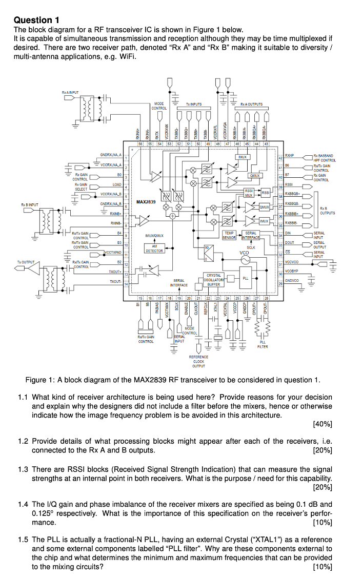
The block diagram for a RF transceiver IC is shown in Figure below. It is capable of simultaneous transmission and reception although they may be time multiplexed if desired. There are two receiver path, denoted Rx A and Rx B making it suitable to diversity multiantenna applications, eg WiFi.
Figure : A block diagram of the MAX RF transceiver to be considered in question
What kind of receiver architecture is being used here? Provide reasons for your decision and explain why the designers did not include a filter before the mixers, hence or otherwise indicate how the image frequency problem is be avoided in this architecture.
Provide details of what processing blocks might appear after each of the receivers, ie connected to the Rx A and B outputs.
There are RSSI blocks Received Signal Strength Indication that can measure the signal strengths at an internal point in both receivers. What is the purpose need for this capability.
The IQ gain and phase imbalance of the receiver mixers are specified as being dB and circ respectively. What is the importance of this specification on the receiver's performance.
The PLL is actually a fractionalN PLL having an external Crystal XTAL as a reference and some external components labelled PLL filter". Why are these components external to the chip and what determines the minimum and maximum frequencies that can be provided to the mixing circuits?
Step by Step Solution
There are 3 Steps involved in it
1 Expert Approved Answer
Step: 1 Unlock

Question Has Been Solved by an Expert!
Get step-by-step solutions from verified subject matter experts
Step: 2 Unlock
Step: 3 Unlock