

Question: Question 2: DFF Below are the DFF logic symbol and circuit diagram (from ic_diagrams.pdf) 14VDD 1CLR 1D 1CLK 1PRE 1Q 1Q PRESET reset D Q
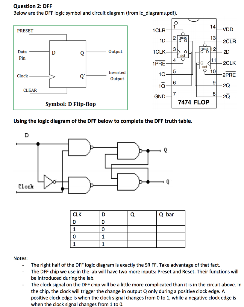
Question 2: DFF Below are the DFF logic symbol and circuit diagram (from ic_diagrams.pdf) 14VDD 1CLR 1D 1CLK 1PRE 1Q 1Q PRESET reset D Q 13 2CLR Output Data Pin Q D 4 2CLK 2PRE 2Q 2Q Inverted Clock Output 8 GND[7 7474 FLOP Symbol: D Flip-flop Using the logic diagram of the DFF below to complete the DFF truth table. Clock a bar CLK 0 0 0 0 Notes The right half of the DFF logic diagram is exactly the SR FF. Take advantage of that fact. - The DFF chip we use in the lab will have two more inputs: Preset and Reset. Their functions wil be introduced during the lab The clock signal on the DFF chip will be a little more complicated than it is in the circuit above. In the chip, the clock will trigger the change in output Q only during a positive clock edge. A positive clock edge is when the clock signal changes from 0 to 1, while a negative clock edge is when the clock signal changes from 1 to 0
Step by Step Solution
There are 3 Steps involved in it

Get step-by-step solutions from verified subject matter experts