

Question: QUESTION 3 [15 MARKS] 2) Design a clamper circuit so that for the input waveform V(t) as given in Figure 4(a), the output waveform
![QUESTION 3 [15 MARKS] 2) Design a clamper circuit so that for](https://s3.amazonaws.com/si.experts.images/answers/2024/05/6647717bbe75a_1396647717b8c710.jpg)
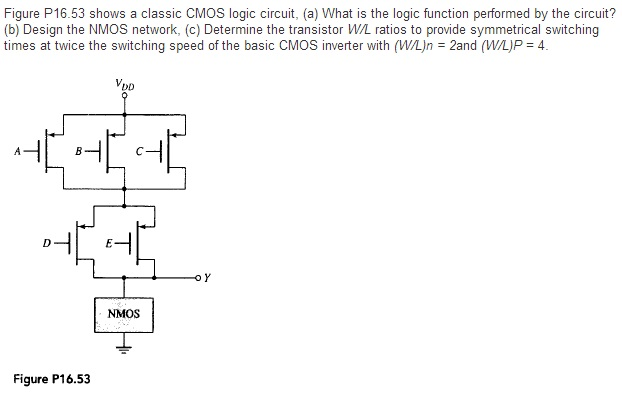
QUESTION 3 [15 MARKS] 2) Design a clamper circuit so that for the input waveform V(t) as given in Figure 4(a), the output waveform (f) as shown in Figure 4(b) can be produced. You shall use ideal diode as part of your circuit design and provide the analysis of your design procedure with the aid of the simplified equivalent circuits. Vi(t) 10V 10V (a) [8 Marks] [CO3, PO3,C3] Figure P16.53 shows a classic CMOS logic circuit, (a) What is the logic function performed by the circuit? (b) Design the NMOS network, (c) Determine the transistor W/L ratios to provide symmetrical switching times at twice the switching speed of the basic CMOS inverter with (W/L)n = 2and (W/L)P = 4. VDD Figure P16.53 NMOS OY
Step by Step Solution
There are 3 Steps involved in it

Get step-by-step solutions from verified subject matter experts