

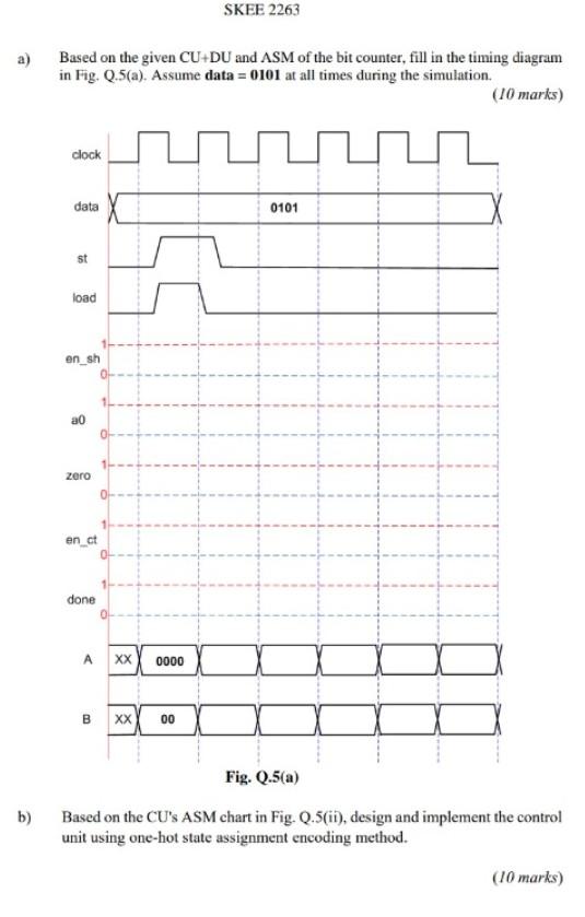
Question: question a, b SKEE 2263 a) Based on the given CU+DU and ASM of the bit counter, fill in the timing diagram in Fig. Q.5(a).
question a,b
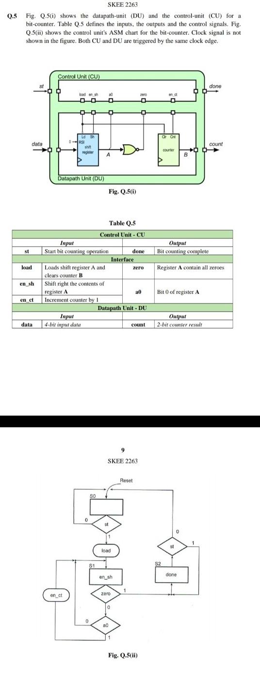
SKEE 2263 a) Based on the given CU+DU and ASM of the bit counter, fill in the timing diagram in Fig. Q.5(a). Assume data = 0101 at all times during the simulation. (10 marks) clock data 0101 st load en_sh a0 zero OP en ct en_ct done XX 0000 xx 00 Fig. Q.5(a) b) Based on the CU'S ASM chart in Fig. Q.5(ii), design and implement the control unit using one-hot state assignment encoding method. (10 marks) SKEE 2263 Q.5 Fig. Q.5(1) shows the datapath-unit (DU) and the control-unit (CU) for a bit-counter. Table 0.5 defines the inputs, the outputs and the control signals. Fig. Q.5(ii) shows the control unit's ASM chart for the bit-counter. Clock signal is not shown in the figure. Both CU and DU are triggered by the same clock edge. Control Unit (CU) st done lead en on ci a0 0 200 . O O Ld Sh 0 RSI ar an data count counter register B Datapath Unit (DU) Fig. Q.5(i) Output Bit counting complete st done load Register A contain all zeroes Table 2.5 Control Unit - CU Input Start bit counting operation Interface Loads shift register A and zero clears counter B B Shift right the contents of register A a0 Increment counter by! Datapath Unit - DU Input 4-bit input data count en_sh Bit 0 of register A en_ct Output 2-bit counter result data 9 SKEE 2263 Reset SO 0 0 s! load S1 S2 done en_sh 1 en_ct zero 0 0 ao Fig. Q.5(ii) SKEE 2263 a) Based on the given CU+DU and ASM of the bit counter, fill in the timing diagram in Fig. Q.5(a). Assume data = 0101 at all times during the simulation. (10 marks) clock data 0101 st load en_sh a0 zero OP en ct en_ct done XX 0000 xx 00 Fig. Q.5(a) b) Based on the CU'S ASM chart in Fig. Q.5(ii), design and implement the control unit using one-hot state assignment encoding method. (10 marks) SKEE 2263 Q.5 Fig. Q.5(1) shows the datapath-unit (DU) and the control-unit (CU) for a bit-counter. Table 0.5 defines the inputs, the outputs and the control signals. Fig. Q.5(ii) shows the control unit's ASM chart for the bit-counter. Clock signal is not shown in the figure. Both CU and DU are triggered by the same clock edge. Control Unit (CU) st done lead en on ci a0 0 200 . O O Ld Sh 0 RSI ar an data count counter register B Datapath Unit (DU) Fig. Q.5(i) Output Bit counting complete st done load Register A contain all zeroes Table 2.5 Control Unit - CU Input Start bit counting operation Interface Loads shift register A and zero clears counter B B Shift right the contents of register A a0 Increment counter by! Datapath Unit - DU Input 4-bit input data count en_sh Bit 0 of register A en_ct Output 2-bit counter result data 9 SKEE 2263 Reset SO 0 0 s! load S1 S2 done en_sh 1 en_ct zero 0 0 ao Fig. Q.5(ii)
Step by Step Solution
There are 3 Steps involved in it

Get step-by-step solutions from verified subject matter experts