

Question: QUESTION THREE ( 2 0 Marks ) ( a ) . What is safe operating area ( SOA ) of power semiconductor devices. ( b
QUESTION THREE
Marks
a What is safe operating area SOA of power semiconductor devices.
b Sketch the curve of safe operating area SOA of power semiconductor and explain the various limitations of the device.
c Sketch the switching characteristics curve of Insulated Gate Bipolar Transistor IGBT and indicate on the curve the switching ON and OFF.
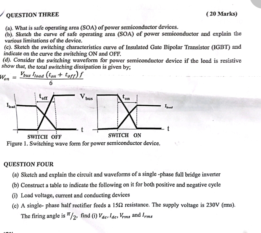
d Consider the switching waveform for power semiconductor device if the load is resistive show that, the total switching dissipation is given by;
Figure Switching wave form for power semiconductor device.
QUESTION FOUR
a Sketch and explain the circuit and waveforms of a single phase full bridge inverter
b Construct a table to indicate the following on it for both positive and negative cycle
i Load voltage, current and conducting devices
c A single phase half rectifier feeds a resistance. The supply voltage is V rms The firing angle is find i and
Step by Step Solution
There are 3 Steps involved in it
1 Expert Approved Answer
Step: 1 Unlock

Question Has Been Solved by an Expert!
Get step-by-step solutions from verified subject matter experts
Step: 2 Unlock
Step: 3 Unlock