

Question: Schematic Figure 1 Procedure 1 . Derive the equation for ( mathrm { V } _ { text { ret } }
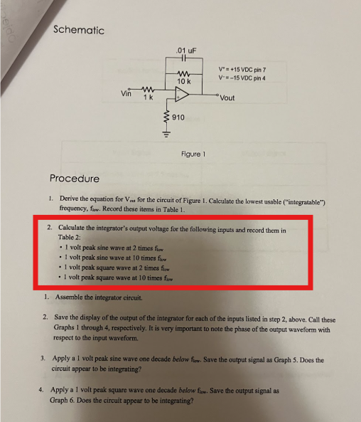
Schematic
Figure
Procedure
Derive the equation for mathrmVtext ret for the circuit of Figure Calculate the lowest usable integratable frequency, mathrmftext fow Record these items in Table
Calculate the integrator's output voltage for the following inputs and record them in Table :
volt peak sine wave at times for
volt peak sine wave at times mathrmftext kve
volt peak square wave at times fisw
volt peak square wave at times mathrmfmathrmic
Assemble the integrator circuit.
Save the display of the output of the integrator for each of the inputs listed in step above. Call these Graphs through respectively. It is very important to note the phase of the output waveform with respect to the input waveform.
Apply a volt peak sine wave one decade below finw. Save the output signal as Graph Does the circuit appear to be integrating?
Apply a volt peak square wave one decade below fice. Save the output signal as Graph Does the circuit appear to be integrating?
Step by Step Solution
There are 3 Steps involved in it
1 Expert Approved Answer
Step: 1 Unlock

Question Has Been Solved by an Expert!
Get step-by-step solutions from verified subject matter experts
Step: 2 Unlock
Step: 3 Unlock